Planar-type avalanche photodiode

a photodiode and avalanche technology, applied in the direction of basic electric elements, electrical apparatus, semiconductor devices, etc., can solve the problems of tunnel dark current liable to generate in the photo-absorption layer, the field strength of the photo-absorption layer in the edge section becomes too high, and the tunnel dark current is liable to increas

Inactive Publication Date: 2001-05-08
RENESAS ELECTRONICS CORP
View PDF12 Cites 38 Cited by
  • Summary
  • Abstract
  • Description
  • Claims
  • Application Information

AI Technical Summary

Problems solved by technology

If the spreading of the voltage over the photo-absorption layer hereat is excessive, however, the field strength of the photo-absorption layer in the edge section becomes too high and passes over the tunneling dark current limit (normally 200 kV / cm) and the dark current of the APD device is increased.
In this case, however, when the bias voltage is spread over the photo-absorption layer in order to bring about the above-mentioned guard-ring effect, there arises another problem that the tunnel dark current is liable to generate in the photo-absorption layer section of the guard-ring because the first setting of the field strength itself is already relatively high.
Accordingly, the conventional planar-type superlattice APD has a problem that a range of the optimum value for the dose of Ti implantation mentioned above tends to become small, depending on the setting of the maximum field strength in the photo-absorption layer.

Method used


Image

  • Planar-type avalanche photodiode
  • Planar-type avalanche photodiode
  • Planar-type avalanche photodiode

Examples


first embodiment

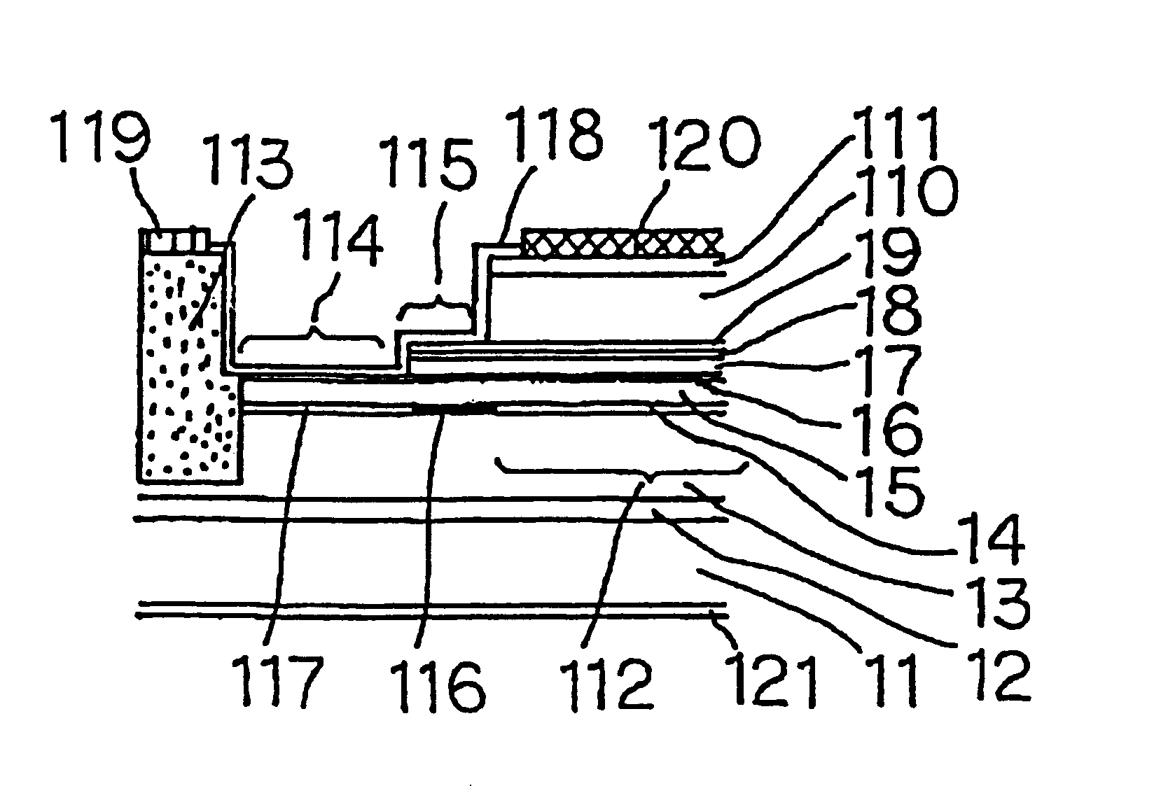
Referring to FIG. 1, a first embodiment is described. Firstly, on a semi-insulating (SI-) InP substrate 11, a p-type buffer layer 12 with a thickness of about 1 .mu.m, a p.sup.- -type InGaAs photo-absorption layer 13 with a thickness of 1.about.1.5 .mu.m, a p.sup.+ -type InP field buffer layer 14 with a thickness of 30.about.100 nm, an undoped InAlGaAs / InAlAs superlattice multiplication layer 15 with a thickness of 0.27 .mu.m, an undoped InP third etching stop layer 16 with a thickness of 10 nm, an n.sup.+ -type InAlAs second cap layer 17 with a thickness of 0.1 .mu.m, an n.sup.+ -type InGaAs second etching stop layer 18 with a thickness of 10 nm, an n.sup.+ -type InP first etching stop layer 19 with a thickness of 10 nm, an n.sup.+ -type InAlAs first cap layer 110 with a thickness of 0.5 .mu.m and an n.sup.+ -type InGaAs contact layer 111 with a thickness of 0.1 .mu.m are grown in succession by the gas-source molecular beam epitaxy (MBE) method.

Next, in a peripheral region of a cir...

second embodiment

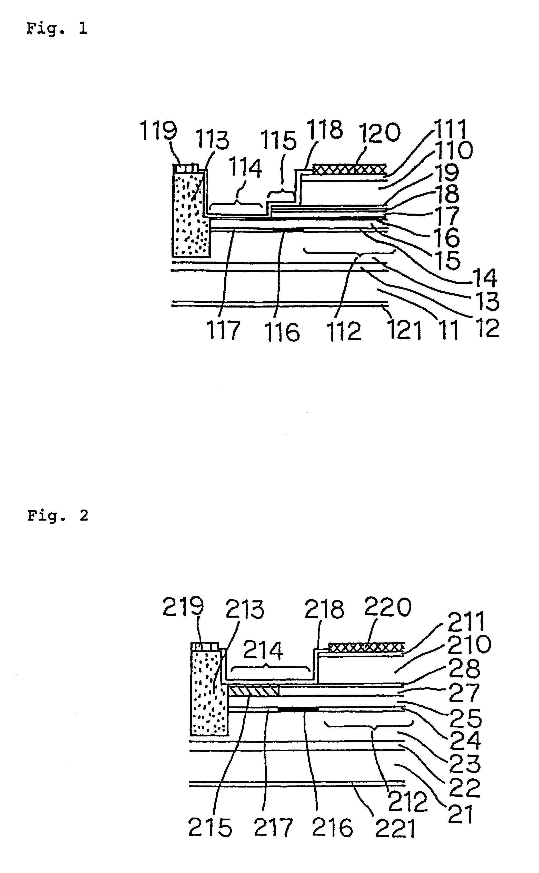
Referring to FIG. 2, a second embodiment is described. Firstly, on a SI-InP substrate 21, a p-type buffer layer 22 with a thickness of about 1 .mu.m, a p.sup.- -type InGaAs photo-absorption layer 23 with a thickness of 1.about.1.5 .mu.m, a p.sup.+ -type InP field buffer layer 24 with a thickness of 30.about.100 nm, an undoped InAlGaAs / InAlAs superlattice multiplication layer 25 with a thickness of 0.27 .mu.m, an n.sup.+ -type InAlAs second cap layer 27 with a thickness of 0.1 .mu.m, an n.sup.+ -type InP etching stop layer 28 with a thickness of 10 nm, an n.sup.+ -type InAlAs first cap layer 210 with a thickness of 0.4 .mu.m and an n.sup.+ -type InGaAs contact layer 211 with a thickness of 0.1 .mu.m are grown in succession by the gas-source MBE method.

Next, in a peripheral region of a circular photo-sensitive region 212 with a diameter of 25 .mu.m, a ring-shaped isolation trench 214 with a width of 3.about.10 .mu.m is formed by selective etching using the etching stop layer 28. There...


PUM


Abstract

With the object of providing a high-speed high-sensitivity planar-type avalanche photodiode (APD) that has high reliability, great manufacturing tolerance and a wide dynamic range, there is presented a planar-type avalanche photodiode, having on a semiconductor substrate a layered structure comprising specific 6 layers, a specific conductive-type acquired region in a peripheral section of a photo-sensitive region and a specific ring-shaped isolation trench region in said photo-sensitive region, wherein a ring-shaped region of the second conductive-type semiconductor cap layer that is inscribed in said ring-shaped isolation trench and located in the periphery of the photo-sensitive region is formed thin to have a thickness equal to or less than the thickness of said semiconductor multiplication layer, and the first conductive-type semiconductor field buffer layer located directly under the ring-shaped cap region, together with a peripheral region in the field buffer layer, is formed to have a lower carrier concentration than the first conductive-type field buffer layer in said photo-sensitive region.

Description

1. Field of the InventionThe present invention relates to a planar-type avalanche photodiode (referred to as APD hereinafter) that has high sensitivity and a wide dynamic range as well as high reliability suitable for use in high-speed optical fiber communication.2. Description of the Prior ArtAs a high-speed high-sensitivity optical receiver for use in the next generation optical fiber communication system, a planar-type superlattice APD shown in FIG. 6 has been reported (IEEE Photonics Technol. Lett., Vol.8, pp.827-829, 1996; Japanese Patent Application No.299996 / 1994 / Japanese Patent Application Laid-open No. 312442 / 1995).In such a device that is a first example of the prior art herein, a higher gain-bandwidth product (GB product) and lower noise are brought about through the enhancement effect of an InAlAs / InAlGaAs superlattice multiplication layer on the ionization rate ratio. At the same time, higher reliability is also produced therein by a structure in which only a stable InP...

Claims


Application Information

Patent Timeline
Patent Type & Authority Patents(United States)
IPC IPC(8): H01L31/102H01L31/107H01L31/09
CPCH01L31/107
Inventor WATANABE, ISAO
Owner RENESAS ELECTRONICS CORP
Why Eureka
Try Eureka