IC interconnect structures and methods for making same

a technology of interconnecting structures and interconnecting elements, which is applied in the direction of semiconductor devices, electrical equipment, semiconductor/solid-state device details, etc., can solve the problems of poor metal step coverage along the edges of contact openings, ineffective metal deposition and photolithographic techniques, and difficult control of wet chemical etch processes typically used with metals

Inactive Publication Date: 2001-06-12
NEWPORT FAB
View PDF9 Cites 132 Cited by
  • Summary
  • Abstract
  • Description
  • Claims
  • Application Information

AI Technical Summary

Problems solved by technology

However, the decreasing depth of focus that accompanies this increase in resolution requires the production of highly planar surfaces during intermediary process steps.
In light of the need for highly planar surfaces, traditional metal deposition and photolithographic techniques become progressively more ineffective as line widths are scaled down and multiple layers of metal are used.
For example, traditional metal deposition techniques can result in poor metal step coverage along the edges of the contact openings.
Furthermore, wet chemical etch processes typically used with metals are difficult to control.
While dry plasma etching may be employed with many metals, other metals with highly desirable properties (e.g., copper and gold) are generally not amenable to dry etching.
This localized pressure creates mechanical strain on the chemical bonds comprising the surface being polished, rendering the chemical bonds more susceptible to chemical attack by the slurry.
Similarly, it is difficult to fill the high aspect ratio dual damascene structures to form plug 104 and wiring 108 with metals.
This and other known methods are unsatisfactory in many respects.
As a result, significant loss of etch stop material is common during the metal CMP process.
First, there is significant dielectric erosion of the etch stop layer due to chemical-mechanical effects of the slurry.
Second, there is often a loss of dielectric material due to post-metal CMP buffing.
The loss of etch-stop material can be quite significant.
Prior art processes are also unsatisfactory in that the etch-stop layer must be formed undesirably thick.
As stated above, this thick etch-stop layer is not uniformly removed or eroded during metal CMP.
The presence of a thick dielectric layer degrades performance in that typical etch-stop materials, such as silicon nitride, have a relatively high dielectric constant, thereby increasing capacitance values between metal lines within a layer.
Similarly, the presence of etch-stop material between the metal layers can degrade performance due to the resulting high capacitance.
Furthermore, the CMP process and any post-CMP cleaning steps have been known to alter the chemical and mechanical properties of the dielectric (which is in direct contact with the slurry and polishing pad), resulting in reduced etch-selectivity during the subsequent trench etching step.
This greatly reduce the efficacy of the etch-stop layer.
Another disadvantage of known techniques relates to the blanket silicon nitride layer typically used over metals such as copper.
As a result, it has been found that blisters and / or bubbles can form between the interface of the silicon nitride and the previous dielectric layer, thus reducing manufacturing yield and adversely affecting long-term reliability.
Moreover, the silicon nitride layer's high dielectric constant tends to increase inter-metal-line capacitance, thus degrading performance with respect to speed, power, and cross-talk.

Method used


Image

  • IC interconnect structures and methods for making same
  • IC interconnect structures and methods for making same
  • IC interconnect structures and methods for making same

Examples


Embodiment Construction

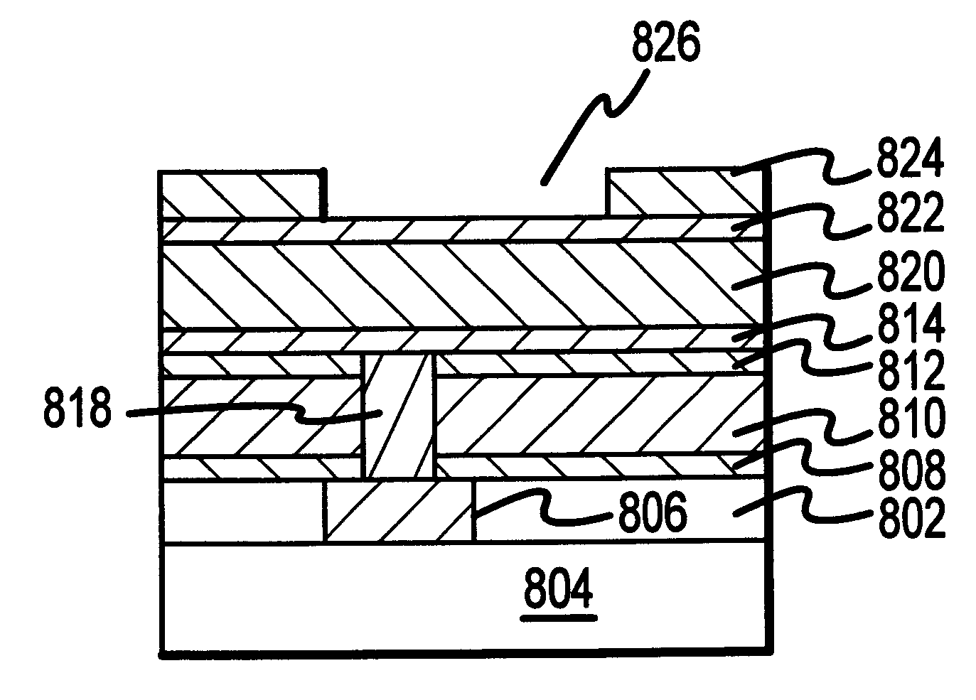
An interconnect fabrication process in accordance with various aspects of the present invention utilizes an etch stop layer deposited after CMP of the previously formed metal wiring or conductive plug layer, thereby eliminating the effect of erosion and allowing a thin etch-stop layer to be used. With momentary reference to FIG. 4I, a single-damascene process is employed wherein a contact plug 410 is formed within dielectric 402 above conductor 406, where conductor 406 may comprise any previous interconnect layer, diffusion, or the like. An etch stop layer 412 is used to form an interconnect wiring layer 420 within dielectric layer 414. In order to assure consistent thickness of interconnect layer 420, the materials used for etch stop layer 412 and dielectric layer 414 are chosen in conjunction with the particular etch process such that the etch rate of etch-stop layer 412 is substantially less than that of dielectric layer 414 during trench etch, and, likewise, is substantially gre...


PUM

PropertyMeasurementUnit
feature sizesaaaaaaaaaa
heightaaaaaaaaaa
widthaaaaaaaaaa

Abstract

Methods and structures are disclosed for advanced interconnects in sub-micron and sub-half-micron integrated circuit devices fabricated using a single damascene process. a dielectric etch-stop layer (e.g., silicon nitride) is deposited subsequent to rather than prior to CMP processing of the previous metallization layer (e.g., the conductive plug). This scheme effectively eliminates the effect of CMP-induced erosion on the etch-stop layer and therefore allows an extremely thin etch stop to be used. Moreover, a high etch-selectivity can be obtained for the trench etch, and all etch-stop material is removed from beneath the interconnect metal, thereby reducing parasitic effects. A patterned dielectric layer is used as a metal cap in place of the standard blanket silicon nitride layer, thus preventing the formation of blisters and bubbles associated with trapped moisture and gasses, and reducing interconnect capacitance.

Description

The present invention relates, generally, to multilevel interconnects used in integrated circuits and, more particularly, to an improved damascene process and structure which utilizes an etch-stop layer deposited after a metal polishing step along with a patterned cap barrier layer.BACKGROUND ART AND TECHNICAL PROBLEMSAdvanced semiconductor processing technology has permitted the fabrication of integrated circuit devices with sub-micron and sub-half-micron features sizes. This trend toward deep submicron technology (i.e., involving feature sizes less than 0.35 microns) has, in turn, driven the need for multilayer interconnects. As a result, circuit performance in the deep submicron regime is increasingly a function of the delay time of electronic signals traveling between the millions of gates and transistors present on the typical integrated circuit chip. Parasitic capacitance and resistance effects resulting from these otherwise passive interconnect structures must therefore be we...

Claims


Application Information

Patent Timeline
Patent Type & Authority Patents(United States)
IPC IPC(8): H01L21/70H01L23/52H01L21/768H01L23/532
CPCH01L21/76807H01L21/76834H01L23/5329H01L2924/0002H01L2924/00
Inventor ZHAO, BINBRONGO, MAUREEN R.
Owner NEWPORT FAB
Why Eureka
Try Eureka