Use of barrier refractive or anti-reflective layer to improve laser trim characteristics of thin film resistors

a thin film resistor and anti-reflective layer technology, applied in the field of thin film resistor laser trim characteristics improvement, can solve the problems of many production wafer lots being delayed, poor laser kerf quality, and inability to accurately measure the laser trim quality of precision thin film resistors. , to achieve the effect of reducing inaccuracy in the behavior of thin film resistor

Inactive Publication Date: 2001-07-10
INTERSIL INC
View PDF12 Cites 61 Cited by
  • Summary
  • Abstract
  • Description
  • Claims
  • Application Information

AI Technical Summary

Benefits of technology

The description and summary above, together with the figures, present the invention's benefits in reducing inaccuracies in behavior of thin film resistors when laser trim is used. Apart from the refractory / barrier metal layer, the thermal barrier / isolation oxide layer and the resistor layer, the number and character of layers of insulating, conducting and semiconducting material may vary without affecting the operation and structure of this invention. Further, the invention's benefits apply across all forms of circuit produced in VLSI semiconductor fabrication, wherever thin film resistors are used and trimmed using laser methods. Finally, any constraints on device silicon and dielectric layer thickness imposed by the laser trim process for thin film resistors are relieved by the invention.

Problems solved by technology

Thus, the quality of laser trim of precision thin film resistors can vary due to constructive and destructive interference of the laser's beam energy with layers above and below the resistor material.
Consequently, many production wafer lots may be delayed due to poor laser trim.
Laser trim quality is subjectively evaluated and some wafer lots are scrapped as a result of poor laser kerf quality, which can vary across a wafer or even across a single die.
As a result of this problem, it may take an operator or an automatic laser trimming machine several cycles of operation, measurement and retrimming in order to trim the resistor to the precise resistance required by the integrated or thin film circuit.
However it provides no solution to the problem posed by precision resistors.

Method used


Image

  • Use of barrier refractive or anti-reflective layer to improve laser trim characteristics of thin film resistors
  • Use of barrier refractive or anti-reflective layer to improve laser trim characteristics of thin film resistors

Examples


Embodiment Construction

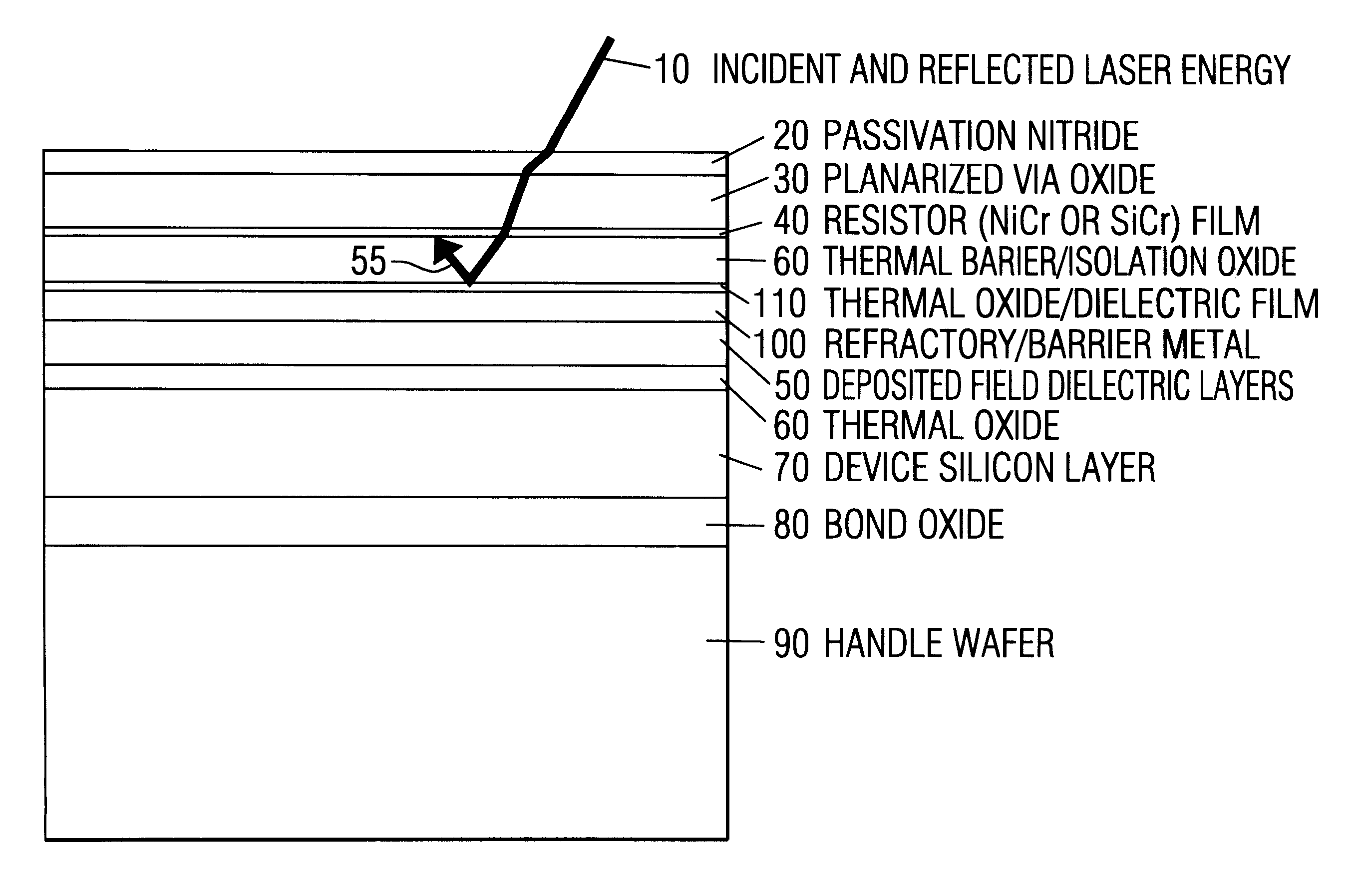
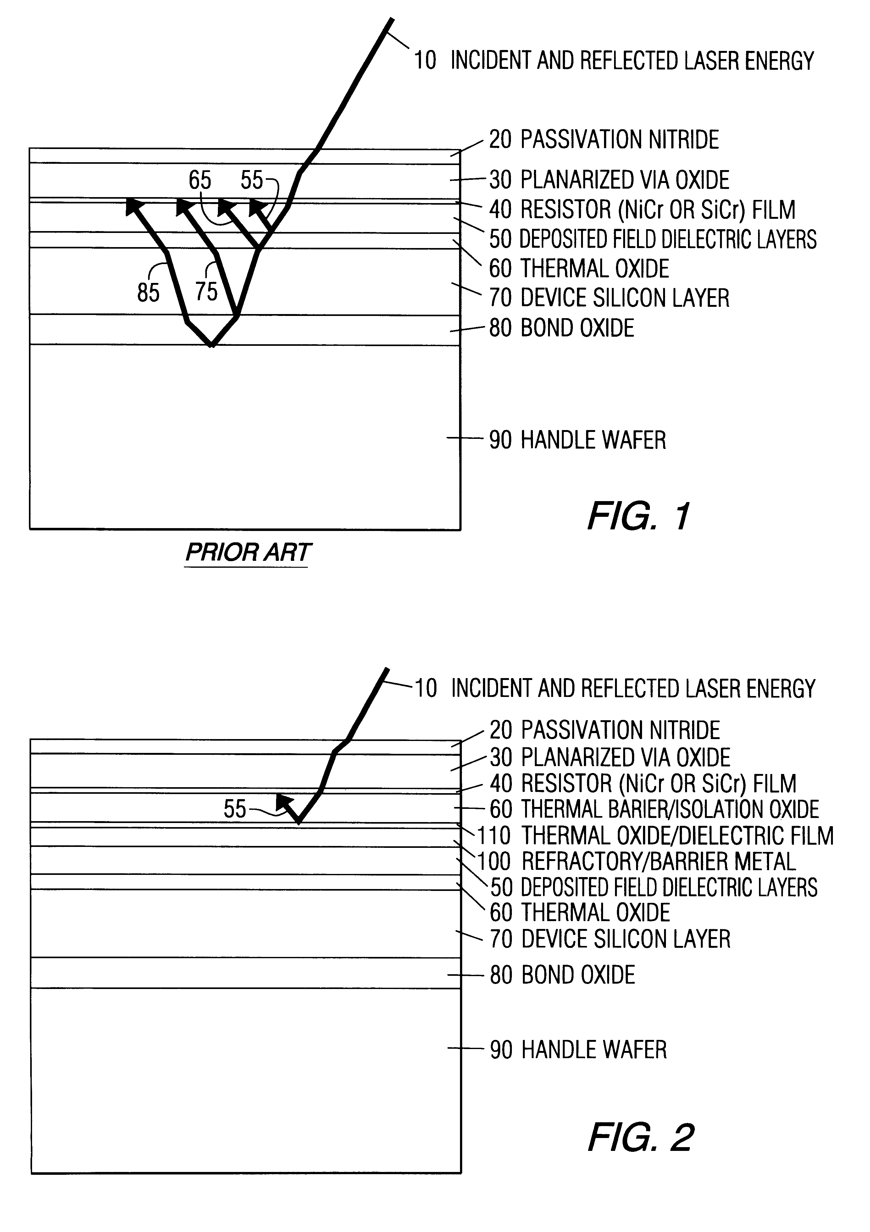
Refer to FIG. 2. The integrated circuit incorporates a device silicon layer 70 which includes one or more semiconductor devices or an integrated circuit. Such devices and integrated circuits and their respective fabrications are conventional. The device substrate 70 may or may not have a handle substrate 90 that is oxide bonded 80 to the backside of the device substrate 70. After formation of the devices or integrated circuit, the devices or integrated circuit are covered with a suitable insulators such as deposited or thermal oxides 50,60. These layers are covered by the refractory / barrier layer 100. In a device made in accordance with the invention such insulator layers are required to separate the devices from refractory barrier metal 100 which may be conductive. The layer 100 is deposited over the substrate and comprises a refractory material such as tungsten, titanium, molybdenum and refractory suicides such as TiSi.sub.2.sup.13,14, CoSi.sub.2.sup.15, MoSi.sub.2, TaSi.sub.2 and...


PUM

PropertyMeasurementUnit
wavelengthaaaaaaaaaa

Abstract

A precision resistor of NiCr or SiCr has a refractive and thermal barrier layer beneath the resistor. The refractive barrier is a layer of refractory metal. The refractory metal prevents the incident laser beam of a laser trimmer penetrating lower layers of the device. Unwanted reflections and refractions caused by lower layers are avoided. The reflective barrier layer is a material selected from the group consisting of tungsten, titanium, molybdenum, TiSi2l3,14, CoSi215, MoSi2, TaSi2 and WSi2.

Description

The invention addresses the general problem of thin film microcircuit resistor fabrication and adjustment, and the specific problem of improving laser trimming to achieve circuit parametric values for such resistors.DISCUSSION OF PRIOR ARTThe technique of laser trimming to bring thin film resistors to their circuit parametric values is well-known in the art. See Elshabini-Riad and Barlow, sections 5.6.4 through 5.6.7, Thin Film Technology Handbook, McGraw-Hill (1998). Current practice requires the tight process control of the thickness and optical properties of layers of the semiconductor wafer that lie below the thin film resistor layer, in an effort to avoid irregularities caused by non-uniform laser energy beam interference.Consider the structure of a typical precision resistor as shown in FIG. 1. It has a silicon handle substrate 90 that is oxide bonded 80 to a silicon device substrate 70. A thermal oxide 60 is grown on the device surface. Layers of deposited dielectric material...

Claims


Application Information

Patent Timeline
Patent Type & Authority Patents(United States)
IPC IPC(8): H01C17/22H01L21/02H01C17/242H01S5/20H01L21/822H01L27/04
CPCH01C17/242H01L28/24B23K26/0048B23K26/0063B23K26/009B23K26/0057B23K2201/40B23K26/0006B23K26/53B23K26/57B23K2101/40B23K2103/16H01S5/20
Inventor MORRISON, MICHAEL J.
Owner INTERSIL INC
Why Eureka
Try Eureka