Technique and process for the imaging and formation of various devices and surfaces

a technology of imaging and surface, applied in the field of process for imaging and surface formation, can solve the problems of unipolar electric field created between two oppositely charged very sharp tip probes, unfavorable and unpredictable variation of devices, and destruction of the surface of the substra

Inactive Publication Date: 2001-07-17
S & F TECHCAL DEV & SOLUTIONS PARTNERS
View PDF14 Cites 41 Cited by
  • Summary
  • Abstract
  • Description
  • Claims
  • Application Information

AI Technical Summary

Benefits of technology

It is a further object of this invention to create an economical way to correct fabrication errors.

Problems solved by technology

An electric field created between two oppositely charged very sharp tip probes, unlike the charged plates, is not uniform, but weakens along a radius perpendicular to a imaginary line connecting the centers of the probes tips.
If energetic short wave particles like x-rays or elections are used to expose the resist to achieve greater resolution, they can destroy the surface of the substrate.
Furthermore, if the substrate is a semiconductor unknown defects in crystalline structure can form allowing for unwanted and unpredictable variations in the devices electrical properties through the thin shell in which the current flows.
This can hamper the goal for current fabrication, which is to create micro devices as small and defined as possible.
This technique can only be used for conducting surface materials and like electron beam lithography could harm the substrates underlying atomic structure.
The first problem is to make smaller devices.
As illustrated above, using the STM may solve this problem, but unlike lithography techniques, STM's can only create the patterns on a chip one at a time, making STM resist exposing very slow and expensive.
The second problem is that as the interconnect wires between transistors get smaller the resistance and capacitance of the circuit increases which creates delays in data transfer.
Finally, another major problem is the heat generated from the formed chips, as they get smaller their power consumption increases as well as the operating electrical currents which can be as high as 50-amps, therefore increasing the device's operating temperature.
As the temperature of the device increases, errors and possible diffusion among the material patterned on the device increases.
Copper, like aluminum, will eventually reach its limit.
Plastic and polymeric fibers are the cheapest to manufacture but are traditionally the worst optically.
The problem associated with the formation of optical interconnects or any optical device is that the creation of optical interconnects is an expensive and fragile process.
The LED's are then bonded to the pre-fabricated silicon circuit, the technique being very time consuming.
However, by doing this, the cost of the manufacturing of a chip increases since the possibility of fab errors and the die size increase.
Having two chips decreases the fabrication cost by using two smaller dies therefore reducing fab errors, but it also decreases the speed of data transfer, called memory latency.
By using optical interconnects instead of standard copper wires, the delay time is significantly reduced, but as with adding more L1 cache the process increases the total cost of the chip.
The disadvantages of using wave-guides are that for operations to be performed the wave-guides may be a few centimeters long.
This takes up valuable space on a two dimensional chip.
An another disadvantage is the lossiness of each operation or cross over.
Lossiness is the leaking of light out of the wave-guide into the surrounding medium, which weakens the signal.

Method used


Image

  • Technique and process for the imaging and formation of various devices and surfaces
  • Technique and process for the imaging and formation of various devices and surfaces
  • Technique and process for the imaging and formation of various devices and surfaces

Examples


Embodiment Construction

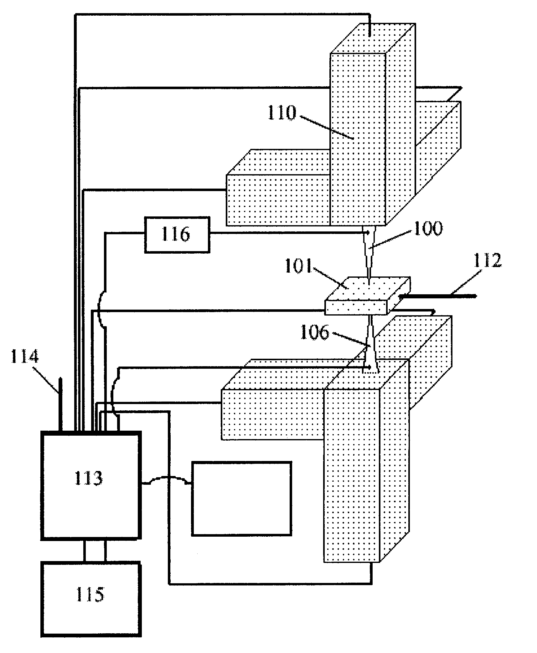
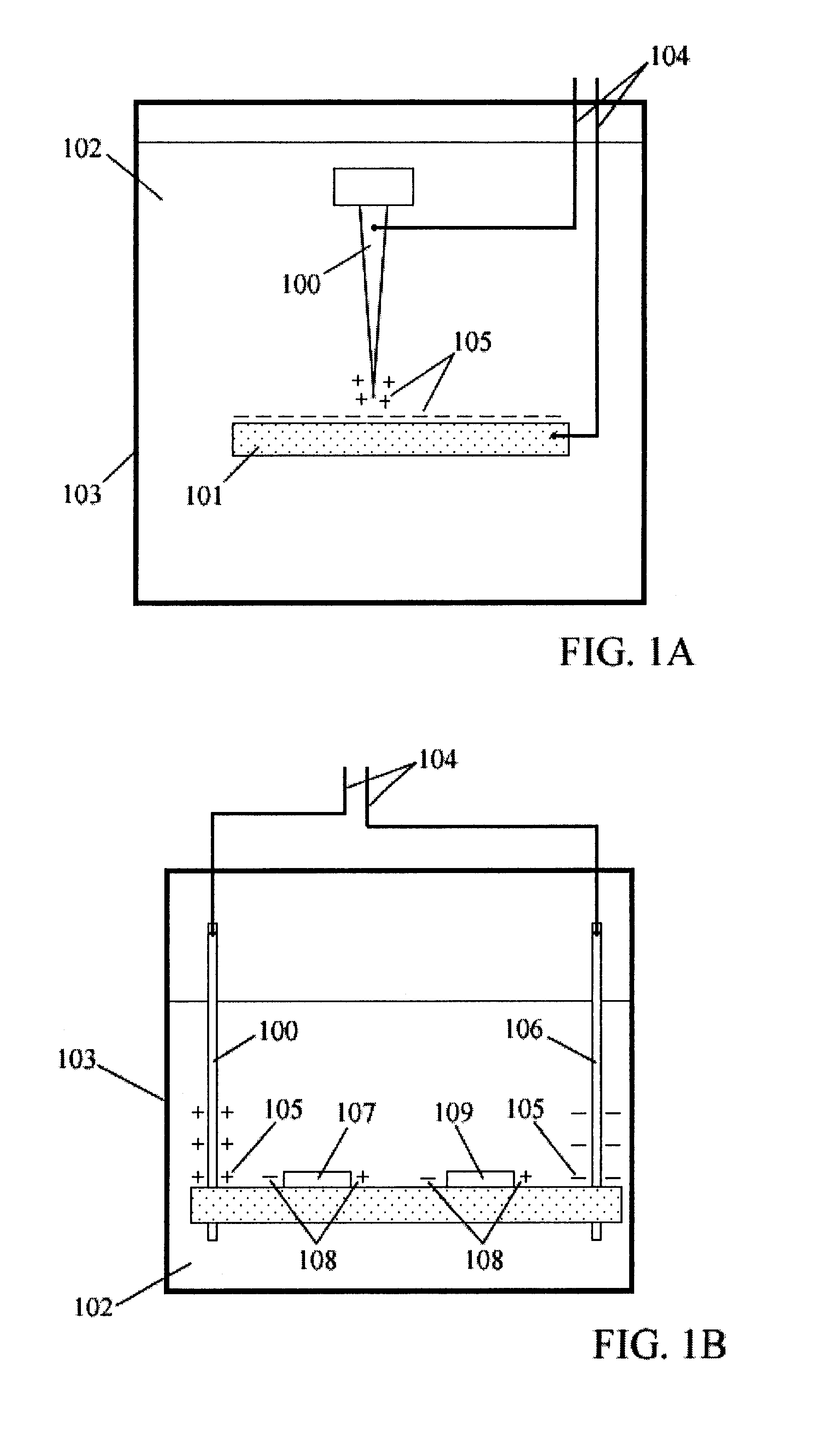
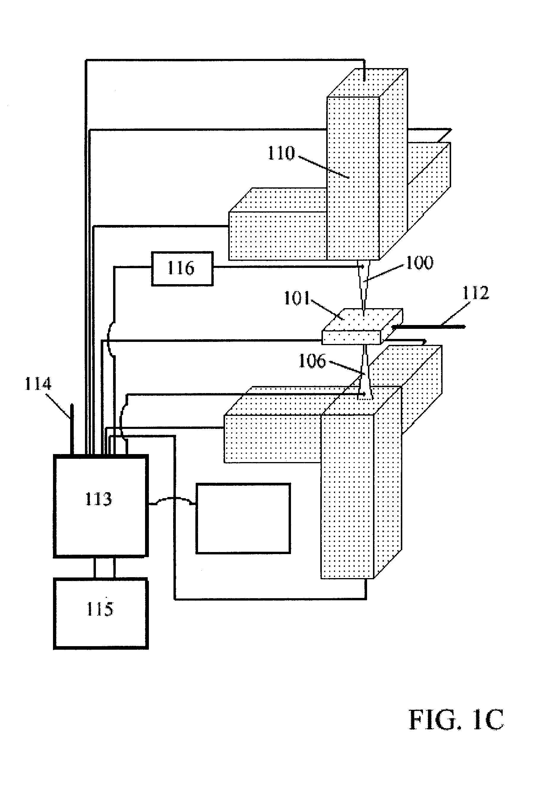
FIG. 1(a) is prior art, in which probe 100 and substrate 101 are submerged in a electrolyte solution 102. A voltage is applied to wires 104, which creates opposite surface charges 105 on probe 100 and substrate 101. The voltage is supplied in a very short pulse. Dependent on the direction of the applied voltage either pits can be created in substrate 101 or material can be deposited on substrate 101, formed by the reduction of ions from solution 102. In this process substrate 101 can not be an insulator, can use cantilever type probes, and can operate within or out of a medium, if used to etch materials.

As used herein, a "substrate" can be any form of soluble or insoluble insulator, semiconductor, polymer, dielectric, or any form of resist; it is the object that is being patterned, patterned on, or existing between the patterned objects. "Material" can be any single or group of elements, molecules, polymers, colloids, or resists that can be transformed, ionized or made into a dipole...


PUM

PropertyMeasurementUnit
temperatureaaaaaaaaaa
thicknessaaaaaaaaaa

Abstract

A technique is described for the formation of nano and micro-scale patterns and optical wave-guides, by using Bipolar Electrochemistry. Atoms are deposited or removed from a surface by creating and moving ions into or out of a medium by the use of electric fields, currents, and induced surface charges. To improve the deposition process, lasers, electron, and ion lenses can be positioned over the surface being deposited to further define the pattern being created. This technique does not harm the surface or crystal lattice of the substrate being deposited on and is powerful enough to transport dopants completely through a substrate. The technique can be used to expose electron beam activated resist which can be used in traditional fabrication processes or to create wave-guides connecting separate optical or electro-optical devices together. As a result smaller and newer types of integrated circuits, electronic devices, and micro machines can be fabricated. The technique can also be used to improve current fabrication processes, the repair of faulty devices, and the imaging of surfaces and hidden dopants.

Description

TECHNICAL FIELD OF INVENTIONThis invention is directed toward a technique for improving the imaging and fabrication of new and traditional types of integrated electrical devices, electro-optical devices, optical devices, and micro machines.BACKGROUND OF INVENTIONUnbound atoms naturally attract or expel electrons forming ions. In general, metal atoms lose electrons most readily becoming positive ions, while nonmetals prefer to gain electrons becoming negative ions. Atoms joined together as molecules can also possess net positive or negative charges. These atoms are called dipoles. Atoms because they contain a positive nucleus and a negative electron cloud can become polarized in an electric field; the atoms in this state are also usually referred to as dipoles. In an electric field the atom can be thought of as possessing two superimposed positive and negative charged regions. Upon the application of the electric field the positive charge nucleus moves in the direction of the applied...

Claims


Application Information

Patent Timeline
Patent Type & Authority Patents(United States)
IPC IPC(8): B82B1/00B82B3/00G01Q60/00G01Q70/06G01Q70/10
CPCB82B1/00B82B3/00B82Y10/00B82Y30/00B82Y40/00H01J2237/31738Y10S977/859Y10S977/857Y10S977/856Y10S977/855Y10S977/874Y10S977/858H01J2237/31747G01Q60/04G01Q60/10G01Q80/00
Inventor ZAFIRATOS, SPYRIDON
Owner S & F TECHCAL DEV & SOLUTIONS PARTNERS
Why Eureka
Try Eureka