High density plasma tool with adjustable uniformity and stochastic electron heating for reduced gas cracking

a plasma tool and uniformity adjustment technology, applied in the field of plasma etching process, can solve the problems of high cost, high precision, and inability to protect other surfaces with lithographically patterned resists, and achieve the effects of high reliability, consistency and manufacturing yield, and high precision of tools

Inactive Publication Date: 2001-07-17
IBM CORP
View PDF5 Cites 55 Cited by
  • Summary
  • Abstract
  • Description
  • Claims
  • Application Information

AI Technical Summary

Problems solved by technology

Such etching processes must generally be performed with etchants which are highly selective to the material (e.g. oxide) to be etched since protection of other surfaces with lithographically patterned resists may not be economically feasible or even possible.
However, the capability to determine the electrical properties of such structures with high reliability, consistency and manufacturing yield as well as acceptable economy is often limited, as a practical matter, by the tools used for processing the semiconductor material, usually in the form of a wafer.
Such tools are often complex and of high precision.
Therefore such tools are generally expensive to build and maintain.
The principal expense of modern production integrated circuits is thus a portion of the cost of the tools used to produce them and, therefore, varies inversely with tool throughput.
Unfortunately, known arrangements for producing a plasma do not provide adequately uniform application of energy or electrical fields to the process gas particularly at high plasma densities.
The problem of process uniformity and high process speed is further complicated and high voltage levels required for high plasma densities by another incident of plasma chemistry referred to as gas cracking.
Therefore, the production of an excess of highly reactive fluorine ions by gas cracking effectively destroys the selectivity required for the process.
Further, since gas cracking is not easily controllable and concentrations of fluorine ions cannot be easily monitored, the repeatability of etching of oxide to a desired thickness is also lost.
Further, the rate at which the process proceeds will vary substantially across the wafer, possibly yielding inconsistent electrical properties of devices on a single chip, and device damage.
However, such tools are not suitable for HDP etching of oxides.
Rather, capacitively coupled parallel plate magnetrons and multi-frequency sources are often used for many advanced oxide etches even though they are incapable of approaching the plasma densities of HDP tools or producing reasonably or acceptably uniform plasma density distributions at more than moderate plasma densities.
However, while all of these asserted qualities are desirable for an oxide etch system as well as other HDP systems, there has been no solution to lack of uniformity of plasma density distribution over an area of practical dimensions for semiconductor processing in production environments, particularly for an oxide etch process.
It can readily be appreciated that such damage, particularly in regard to gate oxides, can dramatically reduce manufacturing yields.

Method used


Image

  • High density plasma tool with adjustable uniformity and stochastic electron heating for reduced gas cracking
  • High density plasma tool with adjustable uniformity and stochastic electron heating for reduced gas cracking
  • High density plasma tool with adjustable uniformity and stochastic electron heating for reduced gas cracking

Examples


Embodiment Construction

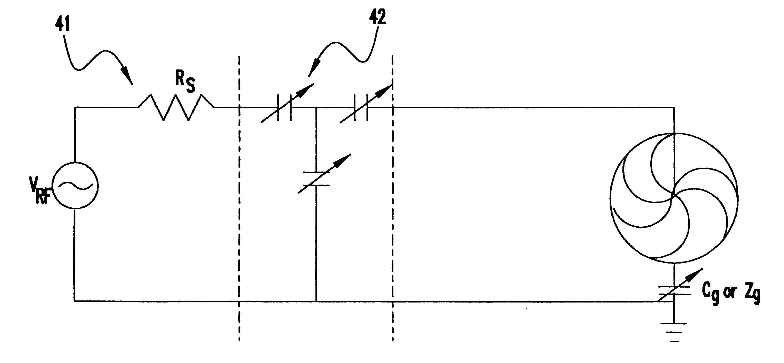
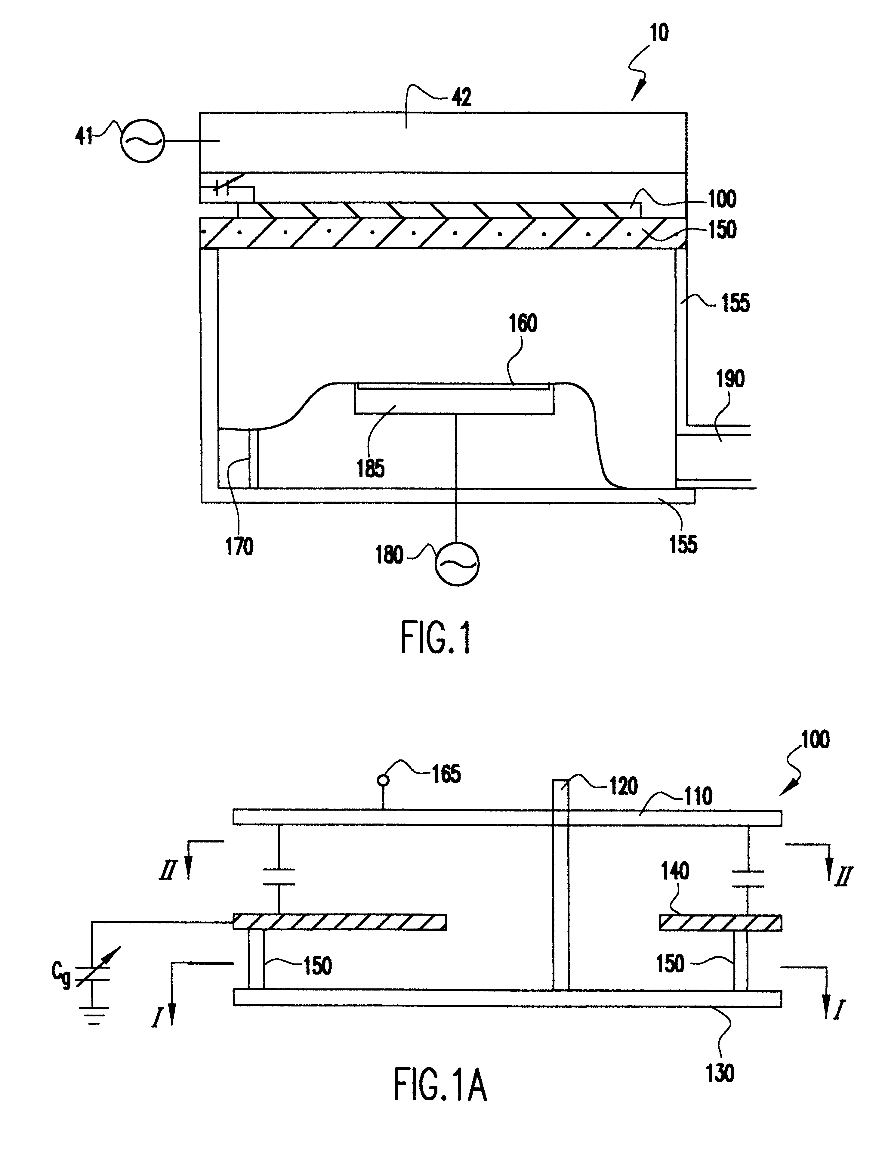
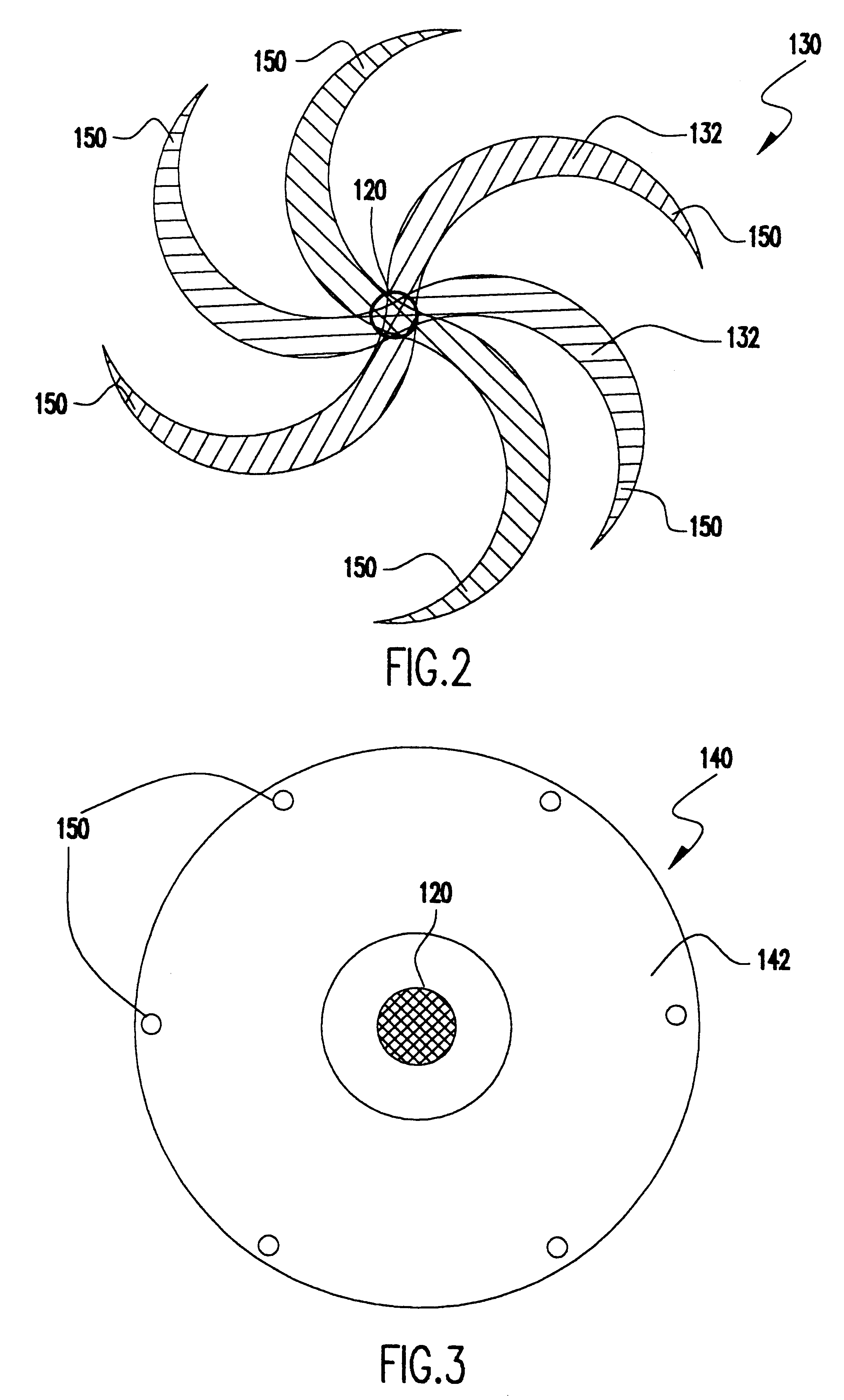
Referring now to the drawings, and more particularly to FIG. 1, there is shown a side, cross-sectional view of a schematic representation of a reaction chamber or vessel 10 in accordance with a preferred form of the invention. It should be understood that the depiction of FIG. 1, being largely schematic, will share many characteristics with known reaction vessels developed for performing various semiconductor wafer processing operations. By the same token, it is to be understood that details thereof are not critical to the practice of the invention. Further, at the level of detail shown in FIG. 1 numerous salient details, particularly involving the antenna arrangement, and elements related thereto of the invention are omitted and, to that extent, the depiction of FIG. 1 can be considered as representing either known systems or the invention in its preferred environment. Accordingly, no portion of FIG. 1 is admitted to be prior art in regard to the present invention.

Reactor vessel 10...


PUM

PropertyMeasurementUnit
frequencyaaaaaaaaaa
plasma densityaaaaaaaaaa
densityaaaaaaaaaa

Abstract

VHF/UHF power having a frequency of about 40 MHz or higher is applied across generally radial elements of an antenna and the phase of a standing wave component of the voltage in the generally radial elements is adjusted to provide relatively uniform density of a high density plasma across an area of at least the size of a semiconductor wafer being processed. Capacitive coupling of power to the plasma enhances the hot tail distribution of electron energies which is associated with low levels of gas cracking and the production of radicals such as fluorine which are not material-selective in semiconductor processing operations such as oxide etching. Accordingly, material-selectivity of processes may be maintained while the high density plasma accelerates the process to significantly improve tool throughput.

Description

1. Field of the InventionThe present invention generally relates to processing of materials with a plasma and, more particularly, to selective plasma etching processes, especially as used in semiconductor device manufacture.2. Description of the Prior ArtThe art of semiconductor electronic device manufacture has become highly sophisticated in recent years to provide a wide range of electrical properties of the devices, often at very high integration density. Generally, device location and basic dimensions of electronic devices included in integrated circuits are defined by a lithographic process and, at the high integration densities currently possible and foreseeable, many subsequent processes are performed in a manner which is self-aligned or material-selective in order to develop structures at sizes smaller than the resolution of lithographic processes and / or avoid problems associated with possible overlay positional errors and mis-registration of plural lithographic patterning p...

Claims


Application Information

Patent Timeline
Patent Type & Authority Patents(United States)
IPC IPC(8): H01J37/32H05H1/46B01J19/08H01L21/302H01L21/3065
CPCH01J37/32082
Inventor KELLER, JOHN H.
Owner IBM CORP
Why Eureka
Try Eureka