

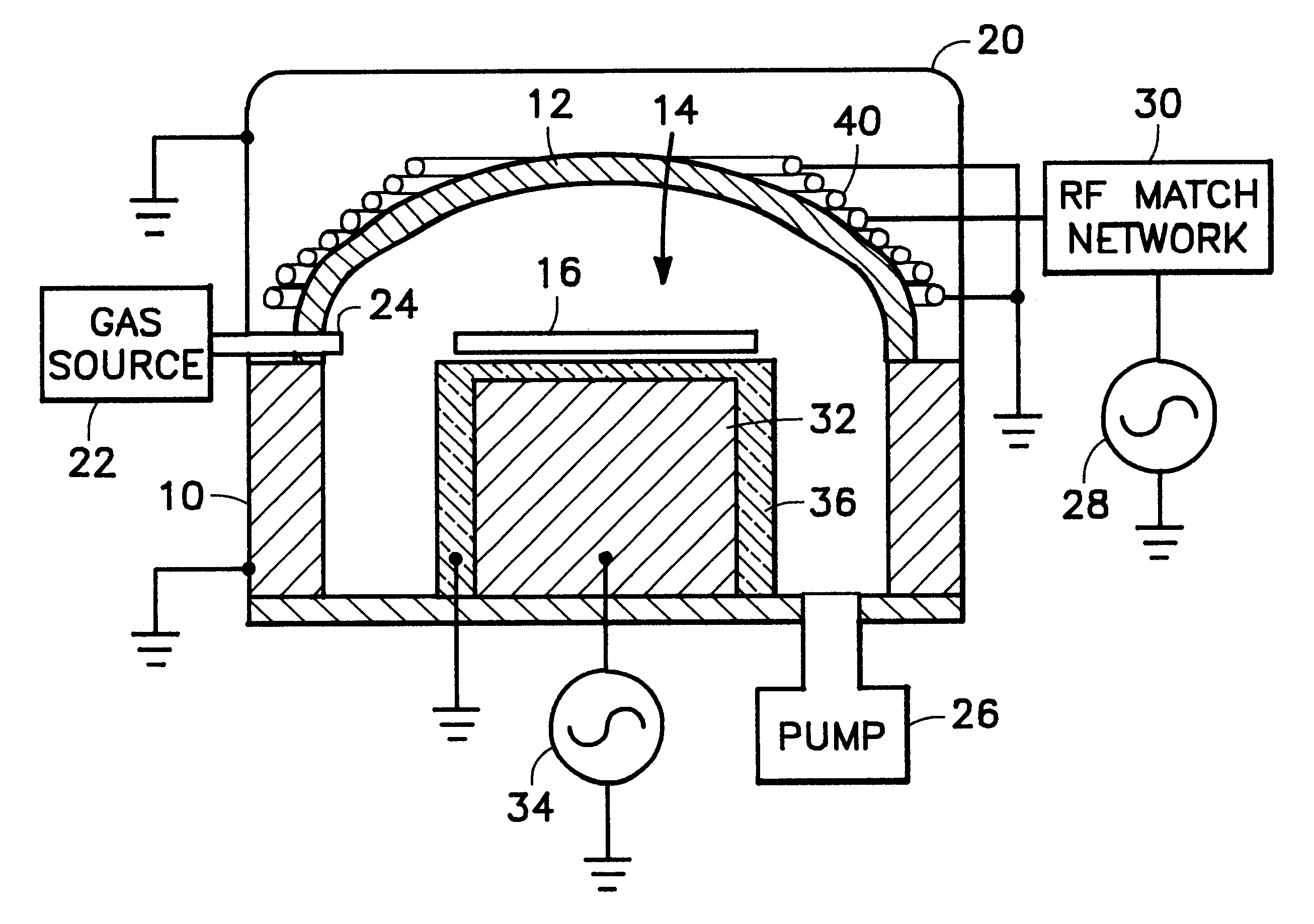
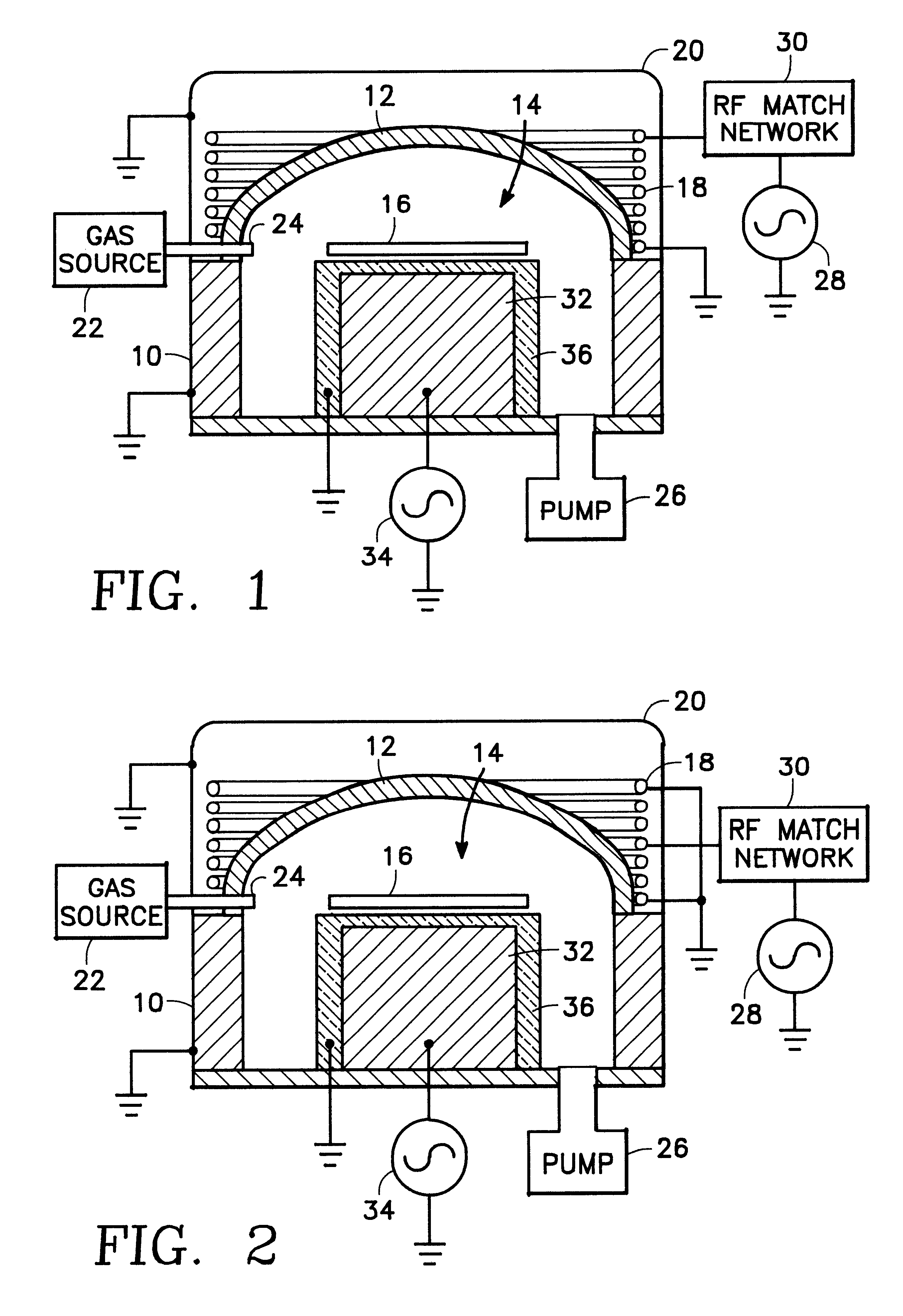
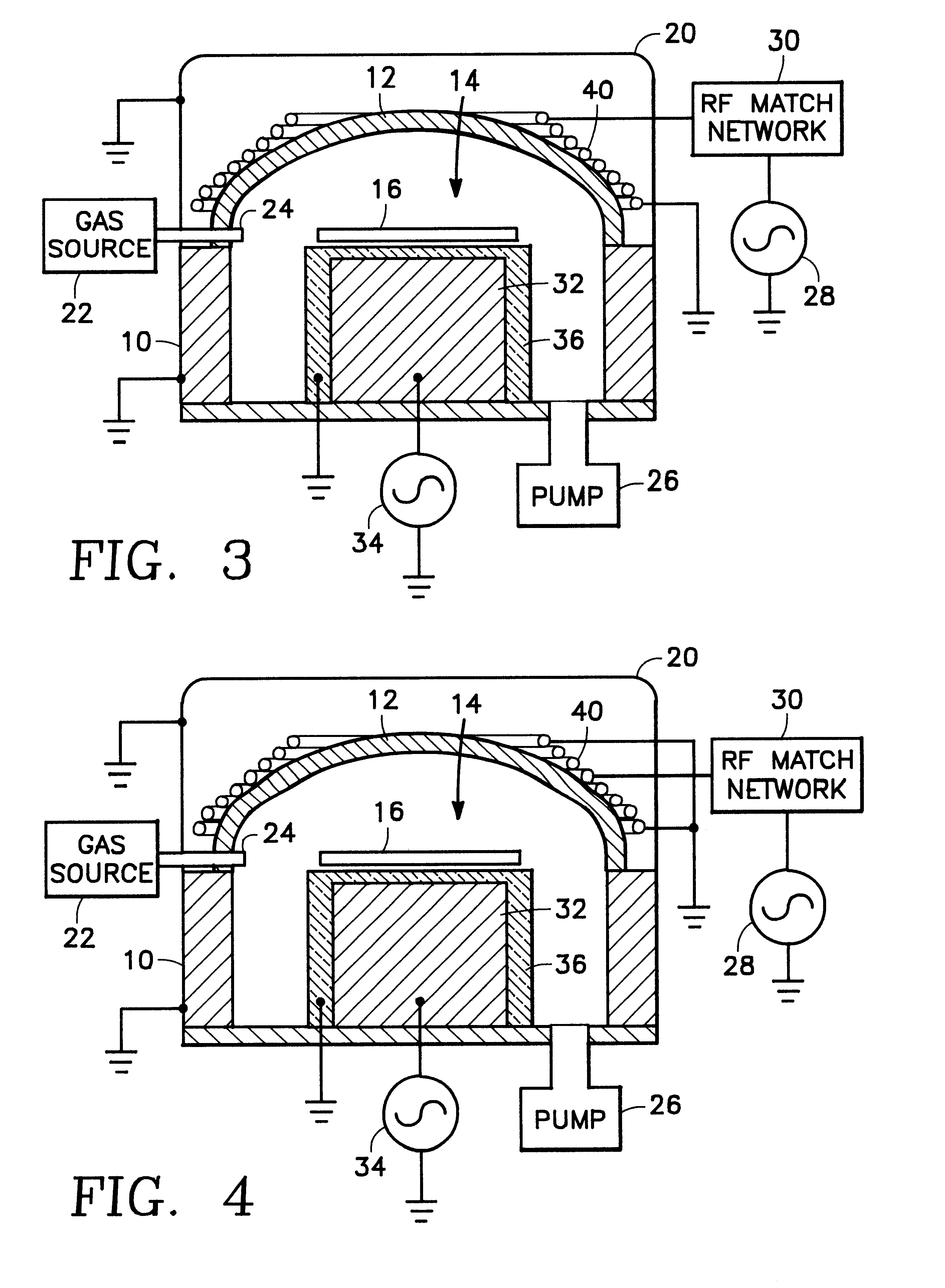
RF plasma reactor with hybrid conductor and multi-radius dome ceiling
a plasma reactor and hybrid conductor technology, applied in the field of radio frequency (r . f.) capacitively coupled plasma reactors, can solve the problems of device damage from charge build-up, etch rate and accumulation of electric charge on the device, and non-uniform spatial distribution of plasma ion density across the wafer surfa
- Summary
- Abstract
- Description
- Claims
- Application Information
AI Technical Summary
Problems solved by technology
Method used
Image

Examples
application-specific embodiments
Although the preferred embodiments of the invention have a much wider range of applicability and therefore are not necessarily application-specific nor limited in application to any particular process, there exist certain embodiments which find their best application to a particular application. Specifically, the particular ranges of the wafer support-to-ceiling height and annular coil mean radius may vary somewhat depending upon the application, for example, to metal etch, polysilicon etch, silicon oxide etch, and so forth. On the other hand, because of the wide process window and wide applicability of the invention, the same reactor embodying the invention including ceiling height and annular coil mean radius dimensions falling within the ranges of the invention as set forth herein may suffice for many or all plasma etch applications (e.g., metal, oxide and polysilicon etch) without requiring modification or substitution, a significant advantage. The purpose of this section of the...
PUM
| Property | Measurement | Unit |
|---|---|---|
| diameter | aaaaa | aaaaa |
| diameter | aaaaa | aaaaa |
| diameter | aaaaa | aaaaa |
Abstract
Description
Claims
Application Information