Ultrafast nanoscale field effect transistor

a field effect transistor and ultra-fast technology, applied in the field of ultra-fast nanoscale field effect transistors, can solve the problems of performance saturation, less rapid performance improvement of logic chips, and the inability to reduce the scale of mosfet below a channel length of approximately 55 nm

Inactive Publication Date: 2001-08-14
IBM CORP
View PDF5 Cites 26 Cited by
  • Summary
  • Abstract
  • Description
  • Claims
  • Application Information

AI Technical Summary

Problems solved by technology

However, recent predictions show that, in its present form with Si as the semiconductor and SiO.sub.2 as the gate insulator, the MOSFET cannot be reduced in scale below a channel length of approximately 55 nm.
This will result in less rapid performance improvement in logic chips, and eventually in performance saturation within a few years, unless significant design or material changes can be implemented within the relevant time frame.

Method used


Image

  • Ultrafast nanoscale field effect transistor
  • Ultrafast nanoscale field effect transistor
  • Ultrafast nanoscale field effect transistor

Examples


Embodiment Construction

The invention described below is a high performance nanoscale field effect transistor (nanoscale FET) designed to be fabricated at scales corresponding to a channel length on the order of 1 nm. Such a scale is considered to be about 1 / 5 of the minimum achievable with conventional metal oxide semiconductor field effect transistor (MOSFET) technology. The inventive nanoscale FET is capable of being fabricated at on-chip densities on the order of 100 times that of current MOSFET devices, and to switch in times on the order of 1 / 100 of current MOSFET devices.

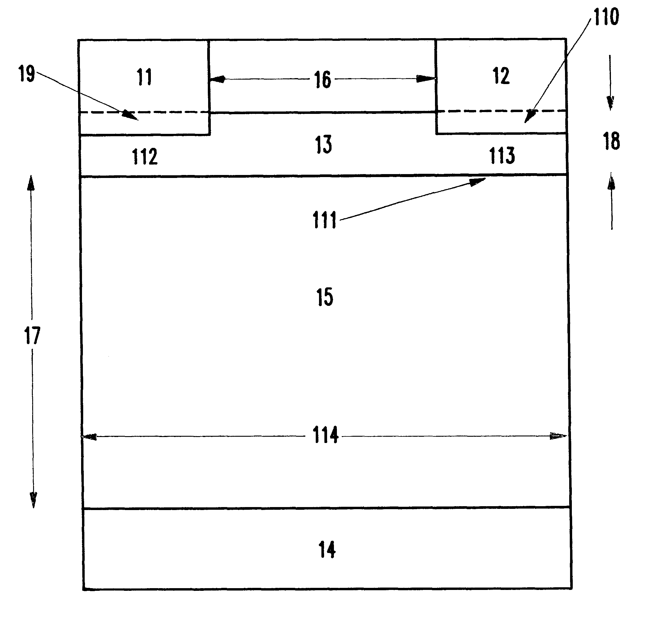
Referring now to the drawings, and more particularly to FIG. 1, one example of the inventive field effect transistor is illustrated. As would be known by one ordinarily skilled in the art, the invention is not limited to the example shown in FIG. 1, but is applicable to any similar device.

In the example shown in FIG. 1, the field effect transistor includes a source region 11, a drain region 12, a channel region 13 extending between ...


PUM


Abstract

A method and structure for a field effect transistor (FET) includes a source region, a drain region, a channel region extending between the source region and the drain region, a gate region, and a gate oxide region separating the gate region from other regions of the FET. The channel region is a Mott insulator. The gate oxide region is thicker than the channel region, and the gate oxide region includes a higher dielectric permittivity than the Mott insulator material.

Description

1. Field of the InventionThe present invention generally relates to field effect transistors (FET's) and more particularly to FET's which are capable of operating properly at nanoscale dimensions.2. Description of the Related ArtThe metal oxide semiconductor field effect transistor (MOSFET) is the universal switching device in current computer logic and memory technology. The on-chip density and speed of MOSFETs has doubled every few years, resulting in the high performance of present day logic and, following Moore's Law, in memory. However, recent predictions show that, in its present form with Si as the semiconductor and SiO.sub.2 as the gate insulator, the MOSFET cannot be reduced in scale below a channel length of approximately 55 nm. This will result in less rapid performance improvement in logic chips, and eventually in performance saturation within a few years, unless significant design or material changes can be implemented within the relevant time frame.The invention descri...

Claims


Application Information

Patent Timeline
Patent Type & Authority Patents(United States)
IPC IPC(8): H01L49/00
CPCH01L49/003H10N99/03
Inventor DONATH, WILM E.NEWNS, DENNIS M.PATTNAIK, PRATAP C.
Owner IBM CORP
Why Eureka
Try Eureka