Method of producing a semiconductor device of SiC

a semiconductor device and selective etching technology, applied in the direction of piezoelectric/electrostrictive devices, microstructured devices, electrical apparatus, etc., can solve the problems of poor directionality of photoelectrochemical etching process, leakage current at the junction between sic and sic conductor at temperatures around 300.degree. c, and achieve good results

Inactive Publication Date: 2001-10-23
CREE SWEDEN
View PDF3 Cites 34 Cited by
  • Summary
  • Abstract
  • Description
  • Claims
  • Application Information

AI Technical Summary

Benefits of technology

According to a preferred embodiment of the invention, the layer to be etched has a doping concentration that is at least 10 times as high as the doping concentration of the adjacent p-type layer. In this way it is secured that in principle all the positive charges required for the etching process will be supplied by the p-ty

Problems solved by technology

One difficulty in the production of piezo-resistive pressure sensors in SiC is the achievement of a diaphragm having the degree of accuracy necessary for accurate pressure measurements.
A drawback with this material system is that the junction between SiC and Si conducts leakage currents at temperatures around 300.degree. C.
Another problem is degradation of the device after a prolonged time due to thermal mismatch effects.
A drawback of this production method is that the photoele

Method used


Image

  • Method of producing a semiconductor device of SiC
  • Method of producing a semiconductor device of SiC
  • Method of producing a semiconductor device of SiC

Examples


Embodiment Construction

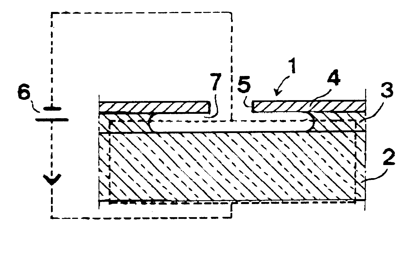
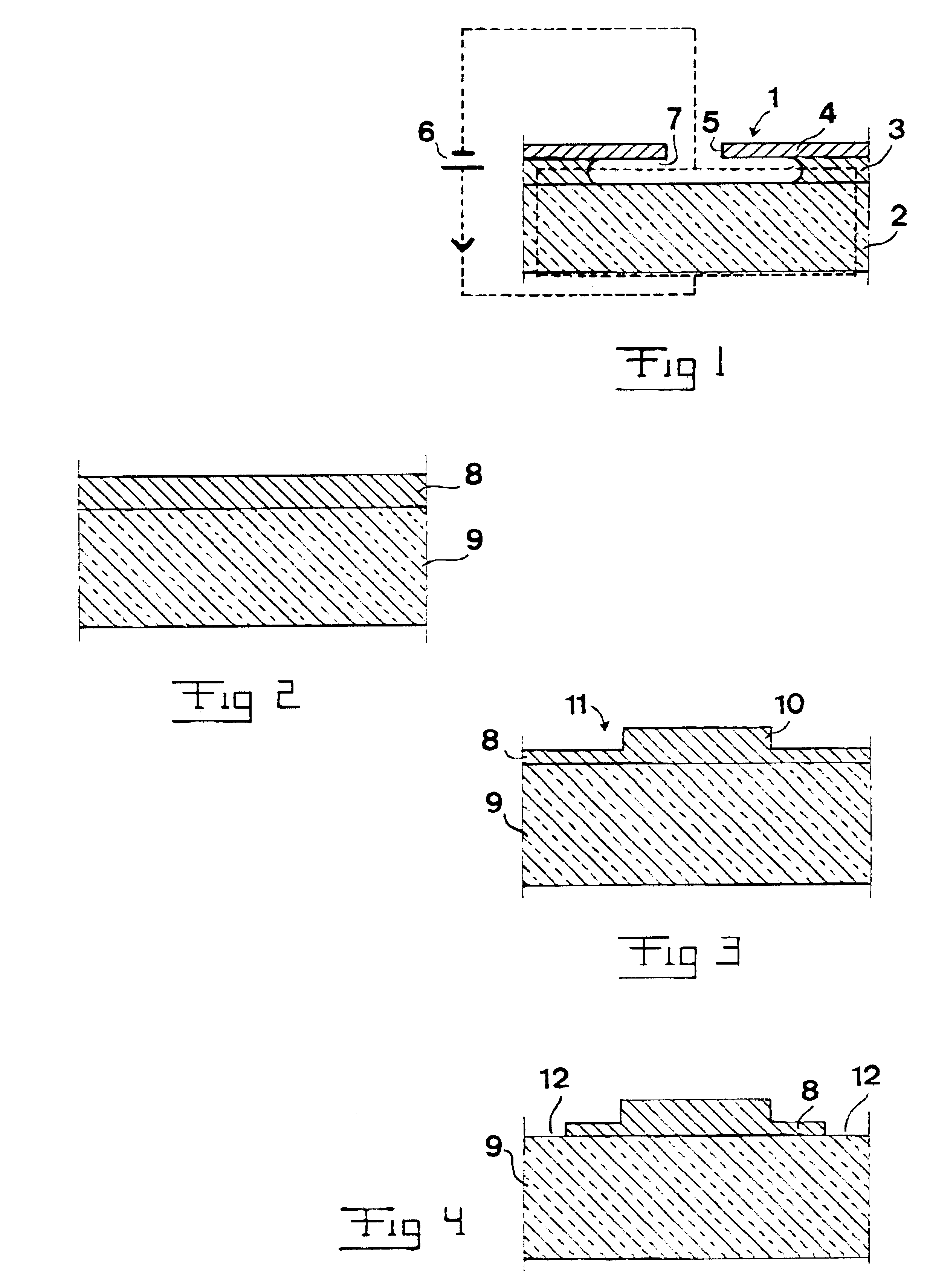
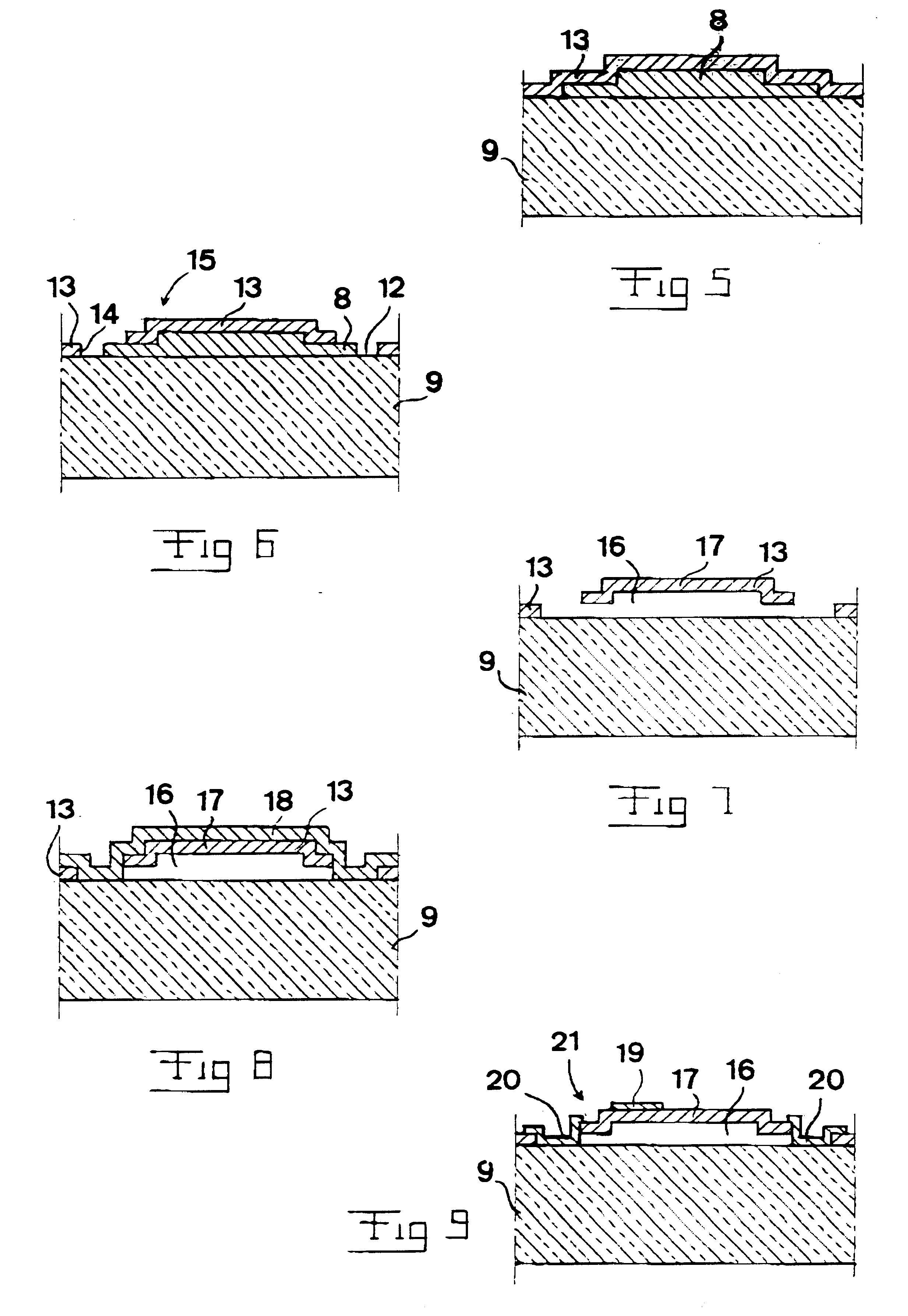
FIG. 1 illustrates in a schematic way a method for etching SiC according to the invention. A multilayer structure 1 of SiC, shown in cross-section in FIG. 1, comprises a first layer 2 of p-type SiC having a first doping concentration, a second layer 3 of p-type SiC being in contact with the first layer 2 and having a second doping concentration, and a third layer 4 of n-type SiC. The doping concentration of the second p-type layer 3 is higher than the doping concentration of the first p-type layer 2. The second p-type layer 3, which constitutes the p-type layer to be etched, is located between the first p-type layer 2 and the third n-type layer 4. In FIG. 1 it is schematically illustrated that an opening 5 is formed in the third layer 4 so as to make it possible to bring the second layer 3 into contact with an etching solution. The first layer 2 is connected to the anode of a source of electric current 6, schematically indicated in FIG. 1, and the multi-layer structure 1 is placed i...


PUM


Abstract

The invention relates to a method for selective etching of SiC, the etching being carried out by applying a positive potential to a layer (3; 8) of p-type SiC being in contact with an etching solution containing fluorine ions and having an oxidising effect on SiC. The invention also relates to a method for producing a SiC micro structure having free hanging parts (i.e. diaphragm, cantilever or beam) on a SiC-substrate, a method for producing a MEMS device of SiC having a free hanging structure, and a method for producing a piezo-resistive pressure sensor comprising the step of applying a positive potential to a layer (8) of p-type SiC being in contact with an etching solution containing fluorine ions and having an oxidising effect on SiC.

Description

TECHNICAL FIELD OF THE INVENTION AND PRIOR ARTThe present invention relates to a method for selective etching of SiC, a method for producing a SiC diaphragm on a SiC-substrate, a method for producing a MEMS (micro electrical mechanical system)-device of SiC having a diaphragm or cantilever structure, and a method for producing a piezo-resistive pressure sensor of SiC.There is a great demand in for instance the automotive industry for low cost, high temperature pressure sensors that can operate in combustion engines. By accurately monitoring and controlling the pressure in the combustion chamber, the engine efficiency can be raised and the fuel consumption and pollutant emission reduced. To meet these needs, new and innovative pressure sensors for high temperature applications are being developed by various research groups around the world.It is well known that silicon carbide (SiC) is a useful material for high temperature applications due to its unique properties, such as its wide ...

Claims


Application Information

Patent Timeline
IPC IPC(8): B81B3/00H01L21/02H01L21/04
CPCB81C1/00595H01L21/0475B81C2201/0114B81C2201/0133
Inventor AD.ANG.S, CHRISTIANKARLSSON, STEFANKONSTANTINOV, ANDREIHARRIS, CHRISTOPHERHORMAN, THOMAS
Owner CREE SWEDEN
Why Eureka
Try Eureka