Integrated circuit chip carrier assembly comprising a stiffener attached to a dielectric substrate

a technology of integrated circuit chip and dielectric substrate, which is applied in the direction of electrical apparatus, semiconductor devices, semiconductor/solid-state device details, etc., can solve the problems of copper oxide degradation, problems of delamination, and two serious problems of particular techniqu

Inactive Publication Date: 2001-12-11
IBM CORP
View PDF44 Cites 71 Cited by
  • Summary
  • Abstract
  • Description
  • Claims
  • Application Information

AI Technical Summary

Benefits of technology

The present invention overcomes various problems of the prior art including eliminating the need for the chemical treatment such as the sodium hypochlorite on the stiffener and power planes on t...

Problems solved by technology

However, this particular technique suffers from two serious problems.
Furthermore, the Vacrel.RTM. reacts with the copper during thermal cycling thereby causing copper oxide to degrade which also results in problems...

Method used


Image

  • Integrated circuit chip carrier assembly comprising a stiffener attached to a dielectric substrate
  • Integrated circuit chip carrier assembly comprising a stiffener attached to a dielectric substrate
  • Integrated circuit chip carrier assembly comprising a stiffener attached to a dielectric substrate

Examples


Embodiment Construction

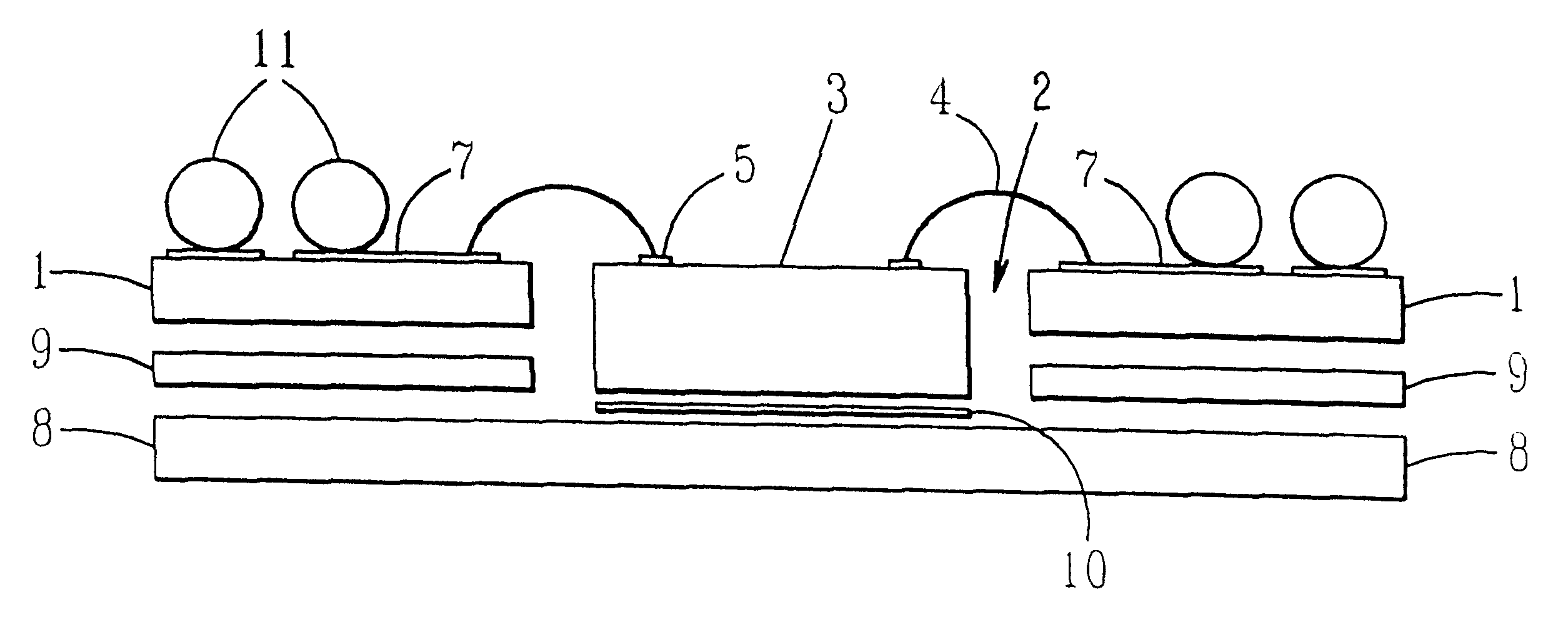
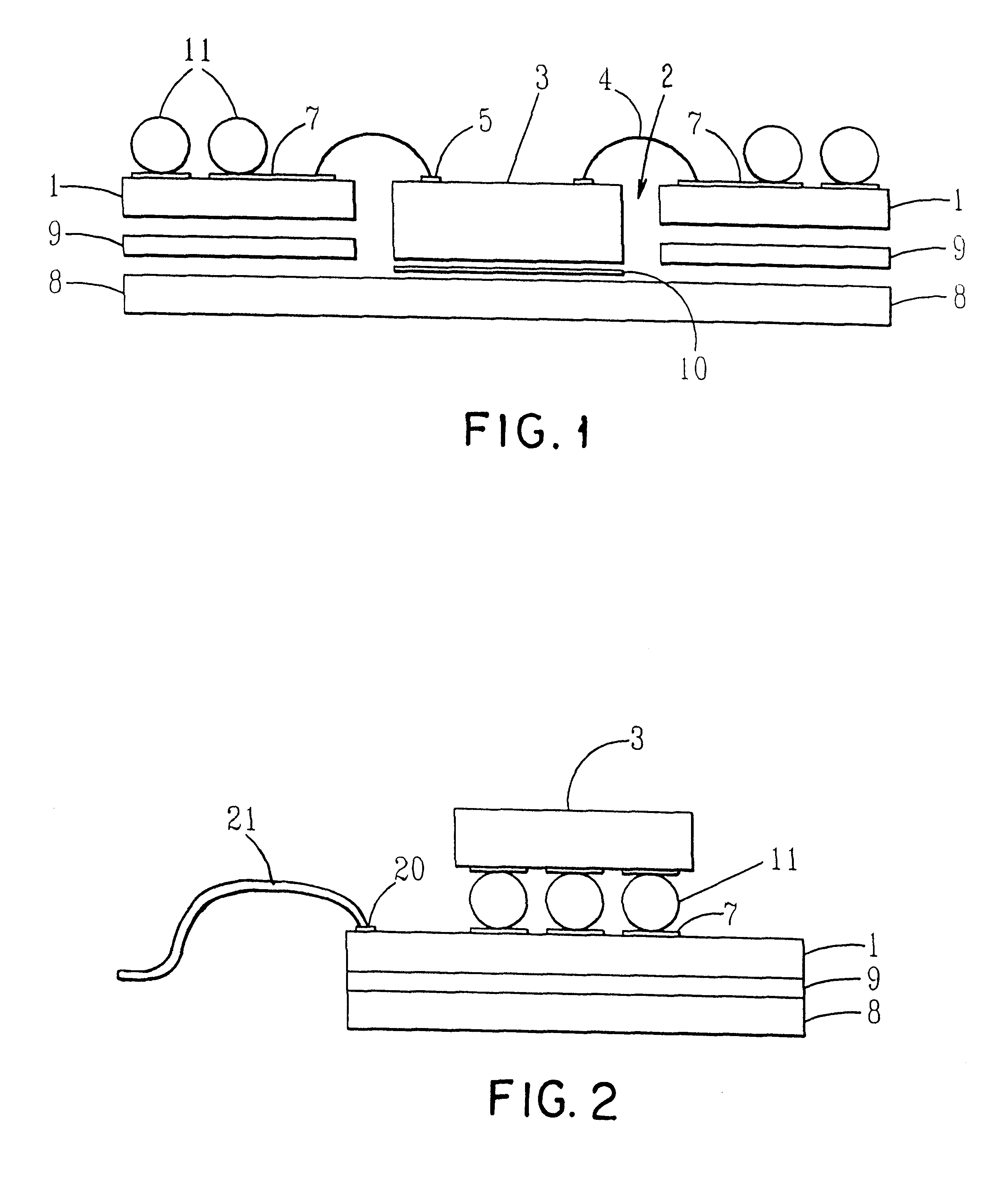
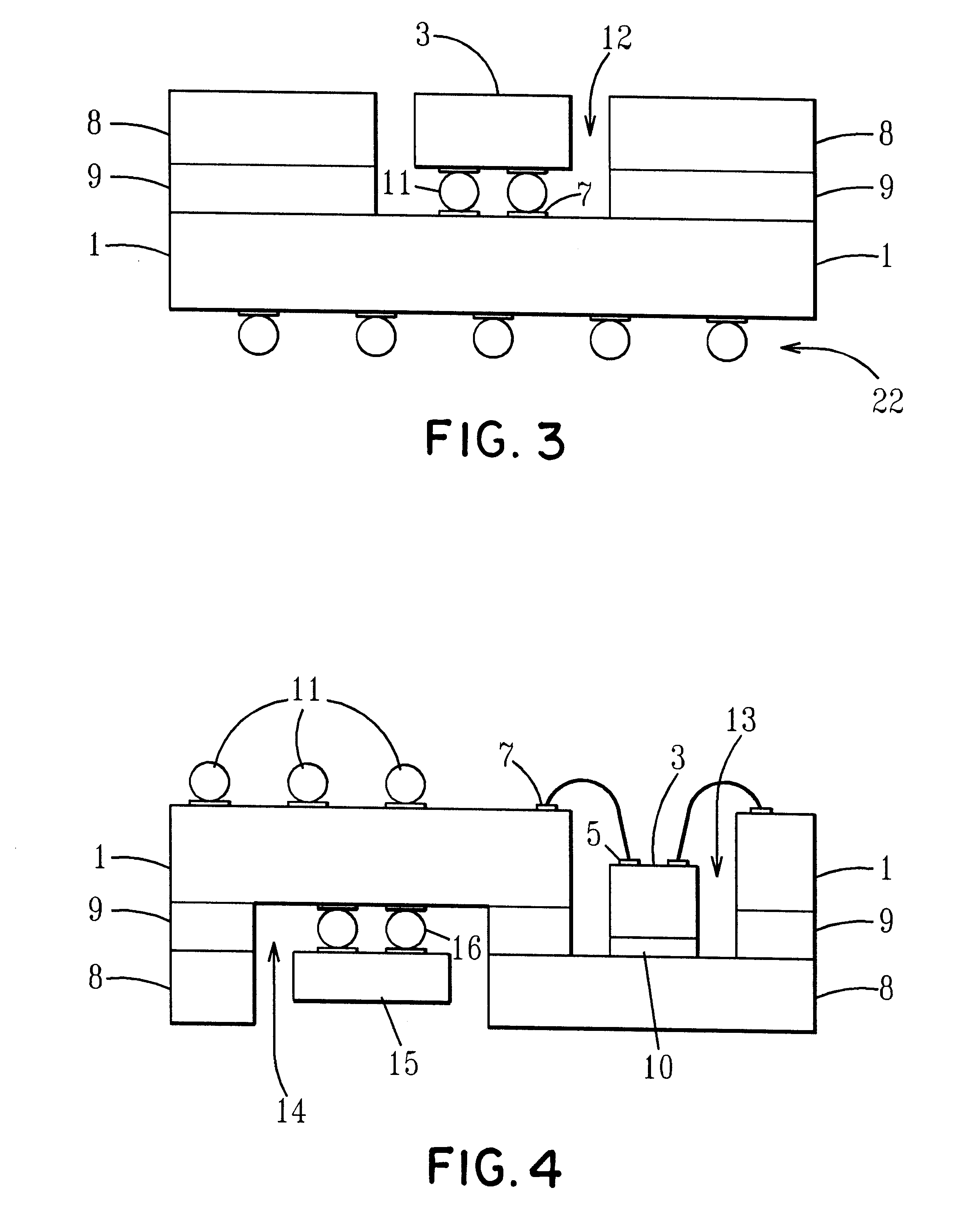
In order to facilitate an understanding of the present invention, reference will be made to the figures wherein the same numeral in different figures represents the same element.

More particularly, FIG. 1 illustrates a cavity down chip carrier package including an integrated circuit chip. Numeral 1 illustrates a laminate circuit element such as a printed circuit board which typically comprises conductive circuitry (not shown) such as copper on both major surfaces of the substrate. The substrate is a dielectric and typically a fiber reinforced polymer composition such as a fiber reinforced epoxy composition, more typically a FR-4 composition including those disclosed in U.S. Pat. Nos. 3,523,037; 4,597,996, disclosures of which are incorporated herein by reference. Other polymers include polyimides such as Upilex SGA available from UBE Ltd., and polytetrafluoroethylene and composites containing polytetrafludroethylene such as Rogers 2800 available from Rogers Corporation.

The conductive...


PUM


Abstract

An integrated circuit chip carrier assembly is provided by joining a substrate having electrically conductive regions on at least one major surface thereof to a stiffener by a bonding film. The bonding film comprises a dielectric substrate having a thermoset adhesive on both of its major surfaces. The thermoset adhesive prior to the bonding is a B-stage adhesive, is tack-free at normal room temperatures and is solvent free.

Description

The present invention is concerned with an integrated circuit chip carrier assembly. More particularly, the present invention is concerned with adhering a laminate chip carrier to a stiffener. Moreover, the present invention is concerned with a method for fabricating the integrated circuit chip carrier assembly.Packaging techniques for integrated circuits have developed with an emphasis on miniaturization. Improved methods enable integrating millions of transistor circuit elements into single integrated semiconductor embodied circuits or chips, and has resulted in increased emphasis on methods to package these circuits in space efficient, yet reliable and mass producible packages. Forming an electronic system requires combining a plurality of integrated circuits and electrically connecting integrated circuits together. Once connected, other devices such as keyboards, video monitors and printers may be connected to and utilized with the electronic system.In order to establish this in...

Claims


Application Information

Patent Timeline
IPC IPC(8): H01L23/52H01L23/498H01L25/065H01L23/48H01L23/538H01L21/58H01L23/13H01L23/12
CPCH01L23/49816H01L23/5387H01L25/0655H01L24/32H01L2224/16225H01L2224/32225H01L2224/48091H01L2224/48227H01L2224/73265H01L2224/83101H01L2224/83856H01L2924/01004H01L2924/01005H01L2924/01011H01L2924/01029H01L2924/01079H01L2924/01082H01L2924/14H01L2924/15153H01L2924/1517H01L2924/15311H01L2924/1532H01L2924/19041H01L2924/00014H01L2924/01006H01L2924/01033H01L2924/01087H01L24/48H01L2924/00H01L2924/181H01L2224/05599H01L2224/85399H01L2224/05573H01L2224/05568H01L2224/45015H01L2924/207H01L2224/45099
Inventor FARQUHAR, DONALD SETONJIMAREZ, LISA JEANINEKLODOWSKI, MICHAEL JOSEPHZIMMERMAN, JEFFREY ALAN
Owner IBM CORP
Why Eureka
Try Eureka