Hybrid circuit and electronic device using same

a hybrid circuit and electronic device technology, applied in the direction of semiconductor devices, semiconductor/solid-state device details, electrical apparatus, etc., can solve the problem of difficulty in increasing the density of devices further

Inactive Publication Date: 2001-12-18
SEMICON ENERGY LAB CO LTD
View PDF1 Cites 50 Cited by
  • Summary
  • Abstract
  • Description
  • Claims
  • Application Information

AI Technical Summary

Benefits of technology

Heat generated by the TFTs can be effectively radiated by forming a heat-radiating layer on the first substrate. Preferably, the heat-radiating layer is made of a material of high thermal conductivity such as aluminum nitride.
The heat-radiating layer can be made of aluminum nitride (AlN). Besides, the layer can be made of aluminum nitride to which oxygen is added, (AlON). In addition, the layer can be made of crystalline compounds of Si, Al, O, and N that are collectively known as SIALON. Further, the layer can be made of AlONC. These materials are effective in relieving the stress between the substrate and the device and controlling the thermal conductivity, and have various features including electrical insulation, high thermal conductivity, heat resistance, and optical transparency.
These materials are effective in relieving the stress between the substrate and the device and controlling the thermal conductivity, and have various features including electrical insulation, high thermal conductivity, heat resistance, and optical transparency.

Problems solved by technology

In spite of these technical trends, it is now difficult to increase the device density further.

Method used


Image

  • Hybrid circuit and electronic device using same
  • Hybrid circuit and electronic device using same
  • Hybrid circuit and electronic device using same

Examples


embodiment 2

The present embodiment gives an example in which the configuration of FIG. 3(A) uses one or more substrates made of a ceramic. All the substrates can be made of a ceramic. Alternatively, the substrate on which TFTs or an SAW device is fabricated may be made of a ceramic. Where a ceramic substrate is employed, there is a wider choice of materials. This is advantageous for productivity and cost.

Where a ceramic substrate is used, it is important to select a substrate having excellent surface flatness. Especially, the substrate on which TFTs are fabricated must be free from pinholes, in addition to having excellent surface flatness.

embodiment 3

The present embodiment gives an example in which the band-pass filter (BPF) consisting of an SAW filter is replaced by an inductor. FIG. 5 schematically shows the construction of the present embodiment. Those parts that are the same as shown in FIG. 3 have the same structures as shown in FIG. 3.

In FIG. 5, conductor patterns 502 form an inductor. A dielectric 501 exists between the successive conductor patterns. A pattern 504 forms one terminal of the inductor and is connected with the output of the invertor consisting of P- and N-channel TFTs. A pattern 503 forms another terminal of the inductor and extends to other components and conductive interconnects (not shown). A substrate 500 is made of a ceramic material.

In this embodiment, an inductor is disposed. Other devices such as chip capacitor, device using a piezoelectric material (e.g., voltage-controlled oscillator (VCO)), and devices exploiting ferrite can be disposed.

embodiment 4

The present embodiment is a modification of the configuration of FIG. 3. The construction of the present embodiment is schematically shown in FIG. 6. The present embodiment is characterized in that an aluminum film 602 is formed on an aluminum nitride film 601. Thus, heat generated by TFTs can be radiated at improved efficiency. This is useful in operating the TFTs at high speeds.


PUM


Abstract

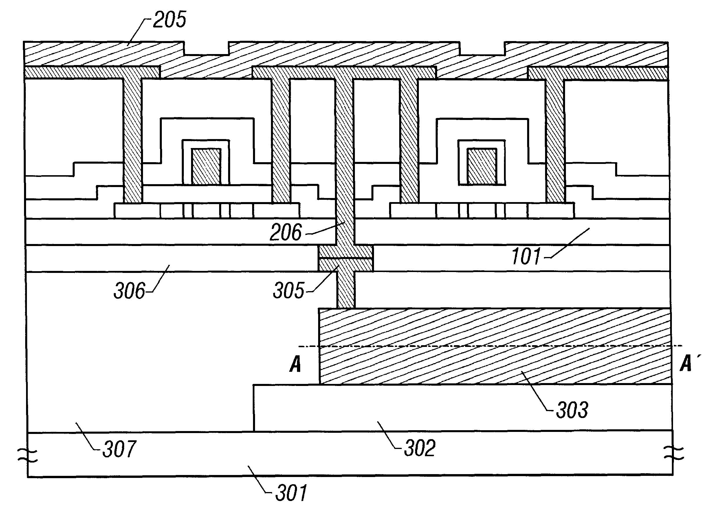
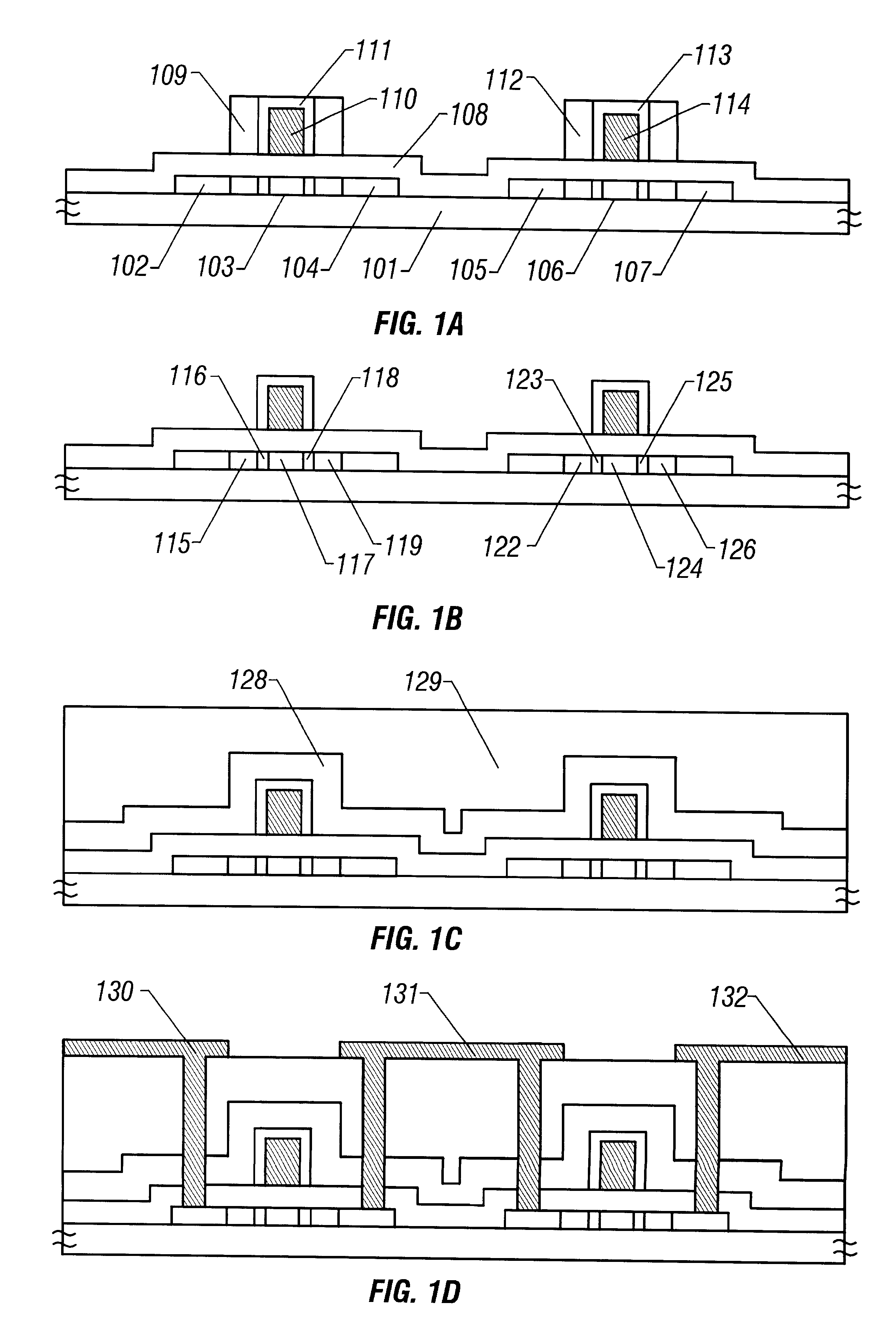
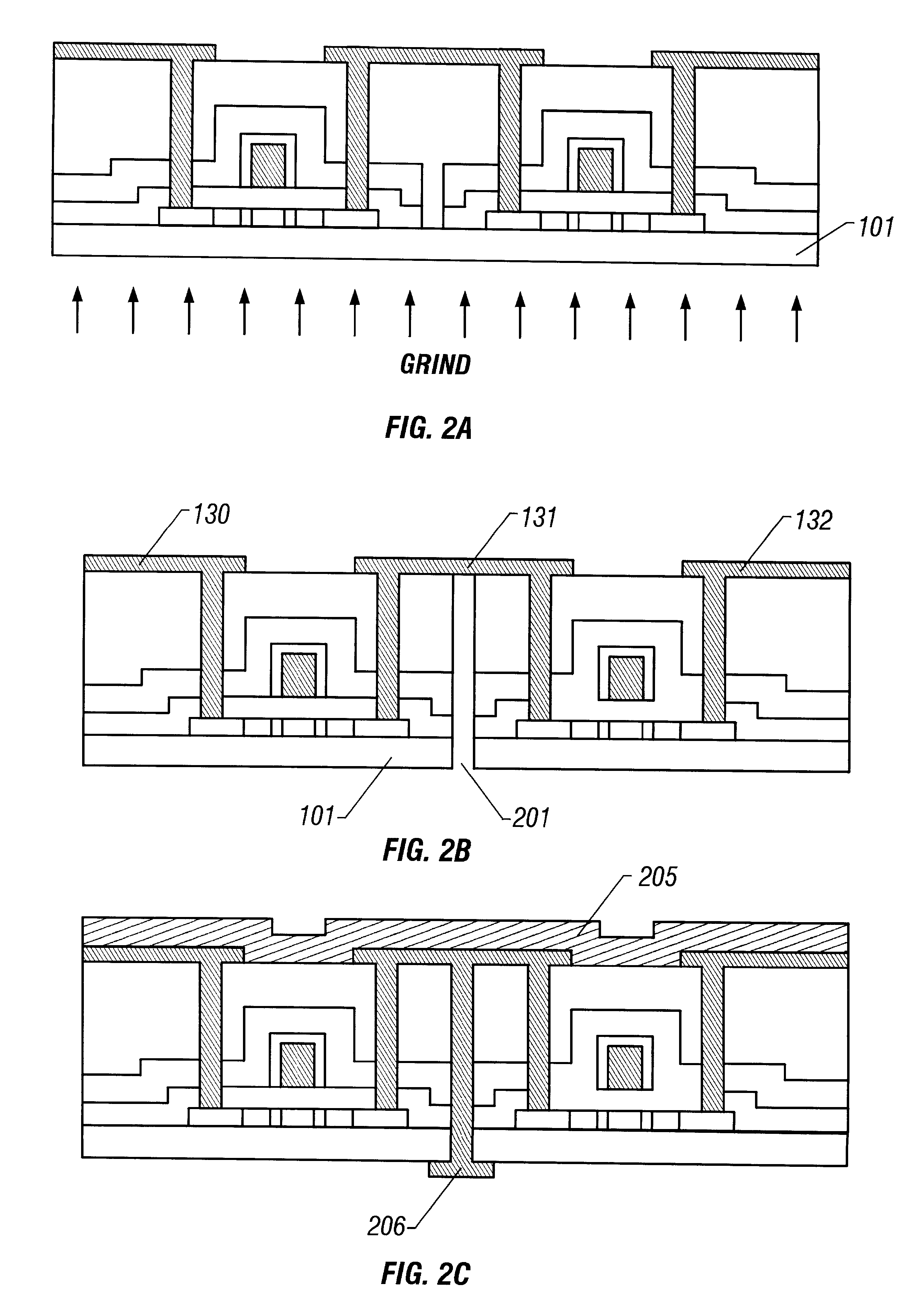
There is disclosed a hybrid circuit in which a circuit formed by TFTs is integrated with an RF filter. The TFTs are fabricated on a quartz substrate. A ceramic filter forming the RF filter is fabricated on another substrate. Terminals extend through the quartz substrate. The TFTs are connected with the ceramic filter via the terminals. Thus, an RF module is constructed.

Description

1. Field of the InventionThe present invention relates to a structure in which thin-film transistors (TFTs) are integrated with a ceramic device or with a ferrite device. The invention disclosed herein can be used in a small-sized, lightweight intelligent terminal typified by a mobile phone, for example.2. Description of the Prior ArtIn recent years, research has been carried out on techniques for fabricating transistors, using a thin silicon film formed on a substrate of quartz or glass. Some of them have been commercialized. These transistors are known as thin-film transistors (TFTs).The main purpose of the research into TFTs is to use them in liquid crystal displays. Such a liquid crystal display has a number of pixels arranged in rows and columns. TFTs are disposed as switching devices at the locations of the pixels. Electric charge held on pixel electrodes is controlled by the TFTs.A still advanced structure that is known has a peripheral driver circuit consisting of TFTs, simi...

Claims


Application Information

Patent Timeline
Patent Type & Authority Patents(United States)
IPC IPC(8): H01L21/70H01L27/12H01L27/06H01L21/84H03H9/05H01L29/66H01L29/786H01L21/77H01L27/13
CPCH01L27/0688H01L27/1203H01L27/13H03H9/0547H01L27/124H01L29/78621
Inventor YAMAZAKI, SHUNPEITERAMOTO, SATOSHI
Owner SEMICON ENERGY LAB CO LTD
Why Eureka
Try Eureka