Power supply control device and method

a control device and power supply technology, applied in the direction of process and machine control, pulse technique, instruments, etc., can solve the problems of large packaging space, poor response of microcomputer basis control to such abnormal current, and failure to opera

Inactive Publication Date: 2002-04-09
YAZAKI CORP
View PDF6 Cites 17 Cited by
  • Summary
  • Abstract
  • Description
  • Claims
  • Application Information

AI Technical Summary

Benefits of technology

The power supply control device further includes overheat protector operating such that when the semiconductor switch is overheated, the overheat protector turns off the semiconductor switch, to thereby protect the semiconductor switch.
Therefore, the power supply control device and method of the invention does not need the shunt resistor, conventionally used, which is connected in series to the power supply path for the current detection. With this feature, the heat loss of the device is suppressed. An abnormal current by a layer short, such as an imperfect short having some short resistance, as well as an overcurrent by a perfect short, can continuously be detected by use of the hardware circuit or the program processing by the MICROCOMPUTER or the like. Further, the overcurrent can be detected without the shunt resistor. Particularly, when the on / off control process for the semiconductor switch is realized by a hardware circuit, there is no need of using the MICROCOMPUTER. This feature brings about the packaging space reduction, and considerable reduction of the device cost.
In a case where, as in the power supply control device, the power supply control device further comprises overheat protector operating such that when the semiconductor switch is overheated, the overheat protector turns off the semiconductor switch, to thereby protect the semiconductor switch, when an imperfect short having some short resistance occurs, the semiconductor switch is repeatedly turned on and off by the controller, whereby the current is greatly varied. That is, in this case, the periodic heating of the semiconductor switch quickens the turning off of the semiconductor switch by the overheat protector. In particular, the power supply control device of the invention can process the abnormal current caused by the imperfect short (layer short), which cannot be processed by any way than the program processing by the MICROCOMPUTER or the like in the conventional device, by using only the hardware circuit contained in the power supply control device per se, or not using the control from an external device, such as MICROCOMPUTER. Therefore, the device circuit is simplified, and hence the device cost is reduced.
In the power supply control device, it is preferable that the semiconductor switch, the reference voltage generating device, the detector, the controller, and the second reference voltage generating device or the overheat protector are formed on one and the same chip. In the ninth power supply control device, the reference current generating device is preferably located outside the chip. By fabricating those means and switch into one chip in an integrating fashion, the device circuit construction is reduced in size, the packing space is reduced, and the device cost is reduced. In the invention, the current detection is based on the detection of a difference between the terminal-terminal voltage of the semiconductor switch and the reference voltage. With formation of the semiconductor switch and the second semiconductor switch on one and the same chip, the invention succeeds in eliminating (removing) common mode error factors which will appears in both the main semiconductor switch and the second semiconductor switch (reference voltage generator) to the almost same extend in the current detecting operation, i.e., adverse influences by power voltage drift and temperature drift, and uneven quality among lots. Additionally, with the feature that the reference current generating device is located outside the chip, the reference voltage (reference current) is made to be insensitive to temperature variation of the chip. Accordingly, high precision current detection is realized.
The power source terminal and the control signal input terminal of the semiconductor switch are connected to the power source terminal and the control signal input terminal of the second semiconductor switch of the reference voltage generating device, respectively. Further, the negative terminal of the second semiconductor switch is connected to the reference current generating device. With such an arrangement, judgement is made as to whether or not current flowing through the power supply path is within a normal range or an abnormal range by comparing a potential at the load terminal of the semiconductor switch with that at the negative terminal of the second semiconductor switch. Thus, the terminals of the semiconductor switch and the second semiconductor switch are commonized. Accordingly, those switches may easily be integrated onto one chip.
In the power supply control device, number-of-times controller adds up the number of times that the control means turns on and off the semiconductor switch, and when the number of on / off control times reaches a predetermined number of times, the number-of-times controller turns off the semiconductor switch. When an overcurrent by a short circuit is detected, the overheat protector quickly functions to make an overheat shut-off (turn off) of the semiconductor switch. In the case of the imperfect short, the semiconductor switch is repeatedly turned on and off. The resultant periodic heating of the semiconductor switch causes the overheat protector to function. Accordingly, it is estimated that time taken till the overheat shut-off is relatively long. In this connection, in the invention, when the number of on / off controls reaches a predetermined number of times, the semiconductor switch is turned off. Therefore, even when the imperfect short occurs, the turning-off of the semiconductor switch may be quickened to a desired turning-off time.

Problems solved by technology

However, those fail to operate when a layer short, e.g., an imperfect short having some short resistance, occurs and small short current flows.
A response of the MICROCOMPUTER basis control to such an abnormal current is poor.
Since the shunt resistor RS, the MICROCOMPUTER 903 and the like are indispensably used in the related power supply control device, a large packaging space is required.
Additionally, those part and component are relatively expensive, so that the resultant device is high in cost.
The resultant periodic heating of the semiconductor switch causes the overheat protector to function.

Method used


Image

  • Power supply control device and method
  • Power supply control device and method
  • Power supply control device and method

Examples


first embodiment

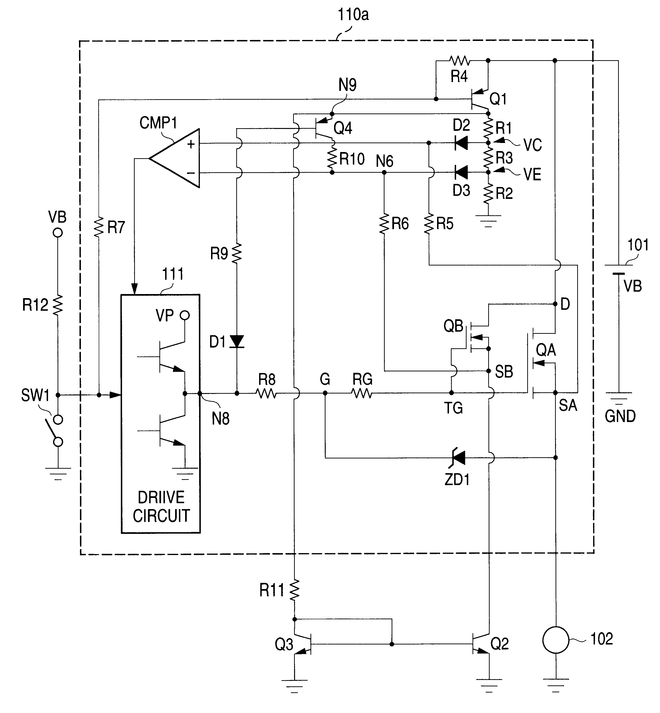
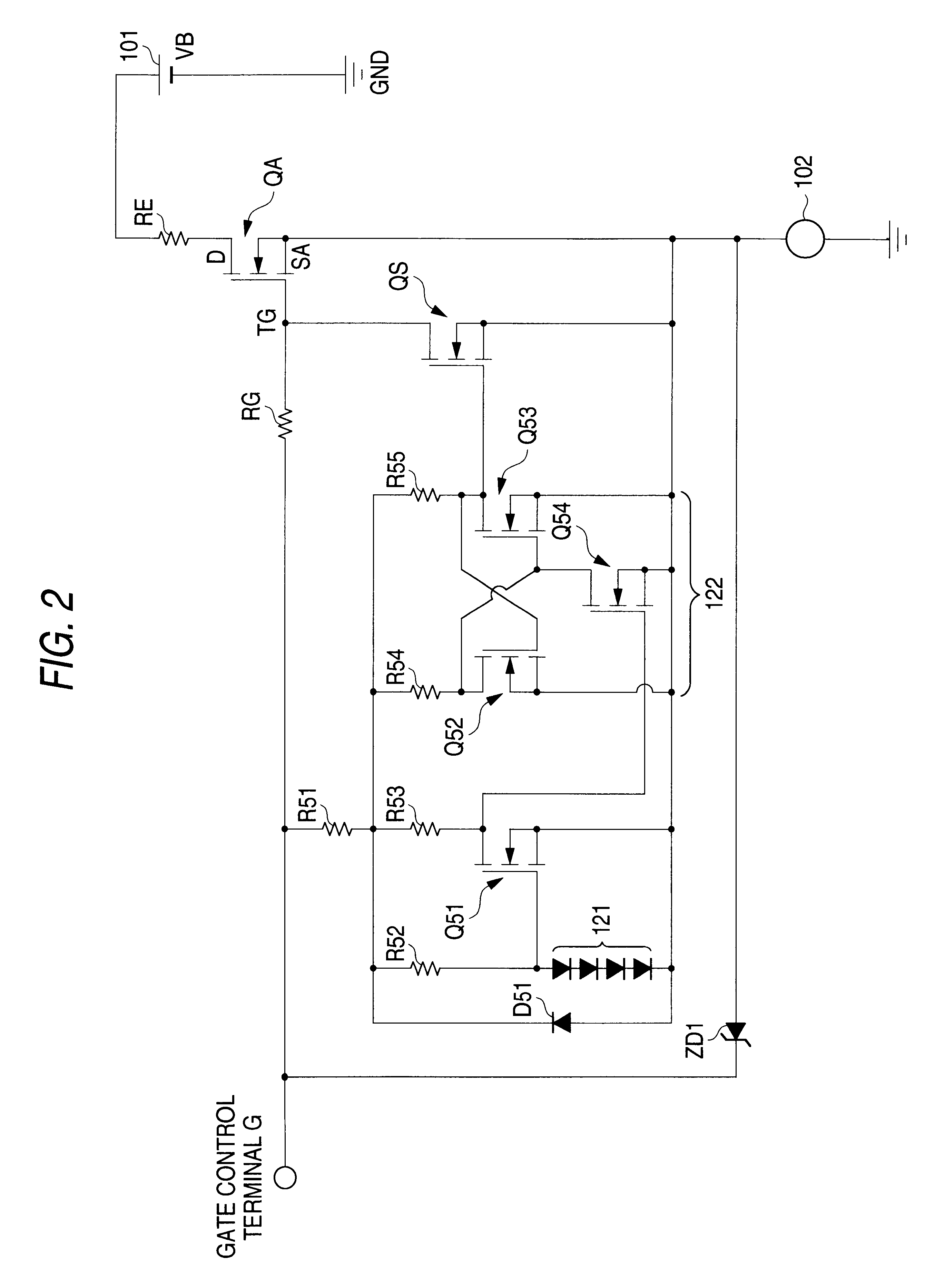
A power supply control device, which forms a first embodiment of the present invention, will be described in accordance with FIG. 1. The power supply control device is arranged such that a drain (D)--source (SA) path of a main control FET QA as a semiconductor switch is inserted in a series fashion in a path for supplying an output voltage VB of a power supply 101 to a load 102. In this instance, the main control FET QA is an NMOS FET having a DMOS structure. If required, it may be a PMOS FET.

In the figure, a circuit section for driving and controlling the main control FET QA includes a reference FET (second semiconductor switch) QB, resistors R1 to R12, and RG, a Zener diode ZD1, diodes D1 to D3, transistors Q1 to Q4, a comparator CMP1, a drive circuit 111, and a switch SW1. In the specification description to follow and the accompanying drawings attached thereto, the resistors are denoted as R followed by reference numerals and characters. Those denotations specifically represent ...

second embodiment

A power supply control device and method, which forms a second embodiment of the present invention, will be described with reference to FIG. 5. The power supply control device of the embodiment is characteristically featured in that the Reference current generating device is constructed as a constant current source. Specifically, difference of the circuit arrangement (FIG. 1) of the power supply control device of the first embodiment is that a resistor R13 is inserted between the resistor R11 and the collector of the transistor Q1 in the Reference current generating device, and a Zener diode ZD2 is connected between the other end of the resistor R13 and ground potential. In FIG. 5, a circuit section 110b enclosed with a dotted line indicates a circuit section to be analog integrated onto a chip (this section will be referred to a chip-circuitry section).

In the circuit arrangement, the collector current IC (Q3) is given by

IC(Q3)={VZD2-(on-voltage of Q3)} / R11

where VZD2 is a Zener volt...

first modification

The first modification is characteristically featured in that a inrush current mask circuit 105 as shown in FIG. 6 is additionally used to the circuit arrangement (FIG. 1 or 5) of the power supply control device of the first or second embodiment.

When the load 102 (e.g., head lights) is turned on, inrush current flows, which is several to several tens times as large as a normal current in amplitude. The period that the inrush current flows depends on the type and capacity of the load 102, but is about 3 msec to 20 msec. If the overcurrent control as described in the first or second embodiment is carried out during the surge-current flowing period, some time is taken till the load is settled down into a stationary state. As a result, the response of the load per se delays sometimes. Specifically, the headlights are delayed in lighting. The embodiment solves this problem by adding the inrush current mask circuit 105 (corresponding to prohibiting device used in claims) to the circuit ar...


PUM


Abstract

When the supply of electric power from a power supply (101) to a load (102) is controlled in a switching manner by a semiconductor switch (QA), reference current generating device (R11, Q2, Q3) generates a reference current, and reference voltage generating device (QB) generates a reference voltage (VDSB) based on the reference current. Detector CMP1 detects a difference between a terminal voltage (VDSA) of the semiconductor switch (QA) and the reference voltage, and the semiconductor switch (QA) is on / off controlled in accordance with the difference between the terminal voltage (VDSA) of the semiconductor switch (QA) and the reference voltage.

Description

1. Field of the InventionThe present invention relates to a power supply control device and method. More particularly, the invention relates to a power supply control device having a semiconductor switch which is controlled in accordance with a control signal supplied to a control signal input terminal to control the supply of electric power from a power supply to a load under the switching control, and a power supply control method in use for the power supply control device.2. Related ArtThe power supply control device with a semiconductor device, which arranged as shown in FIG. 8 is known. This power supply control device, which is used in a vehicle, selectively supplies electric power source from a battery to respective loads, and controls the power supply to the load.As shown, the related power supply control device is arranged such that a shunt resistor RS and a drain (D)--source (S) path of a thermal FET QF are connected in series in a power supply path for supplying an output...

Claims


Application Information

Patent Timeline
Patent Type & Authority Patents(United States)
IPC IPC(8): H03K17/082H03K17/08G05F1/10H02J1/00G05F1/56
CPCH03K17/0822H02M2001/0009H03K2017/0806H02M1/0009
Inventor OHSHIMA, SHUNZOU
Owner YAZAKI CORP
Why Eureka
Try Eureka