Method to fabricate RF inductors with minimum area

a technology of inductors and inductors, applied in the direction of solid-state device manufacturing, electric devices, semiconductor/solid-state device manufacturing, etc., can solve the problems of large parasitic capacitance, adversely affecting both inductance and q factor, and more challenges for resistors than either resistors

Inactive Publication Date: 2002-05-14
CHARTERED SEMICONDUCTOR MANUFACTURING
View PDF7 Cites 58 Cited by
  • Summary
  • Abstract
  • Description
  • Claims
  • Application Information

AI Technical Summary

Problems solved by technology

When considering methods of forming such passive components, however, inductors pose more challenges than either resistors or capacitors.
Conventional planar inductors suffer from several disadvant

Method used


Image

  • Method to fabricate RF inductors with minimum area
  • Method to fabricate RF inductors with minimum area
  • Method to fabricate RF inductors with minimum area

Examples


Embodiment Construction

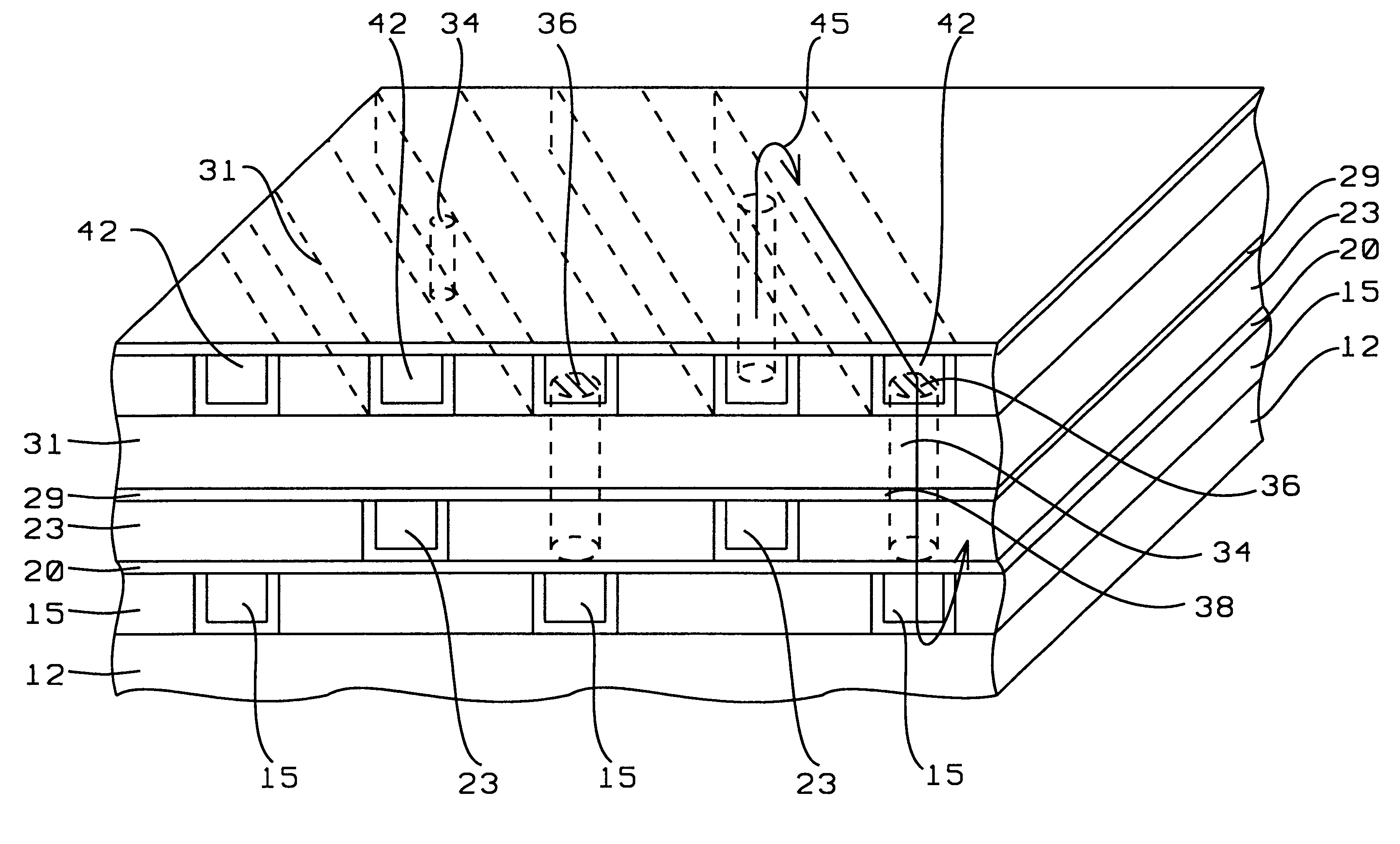
: Copper Damascene Coil Segments

If the metal segments comprising the helical RF inductor of the present invention are to be formed of copper, it is often advantageous to form them within lined trenches, said liner acting as a barrier to prevent the out-diffusion of the copper into the IMD layers. Such formations are called copper damascene formations and the method of their use in the fabrication of the helical inductor of the present invention can be seen by referring to the following figures.

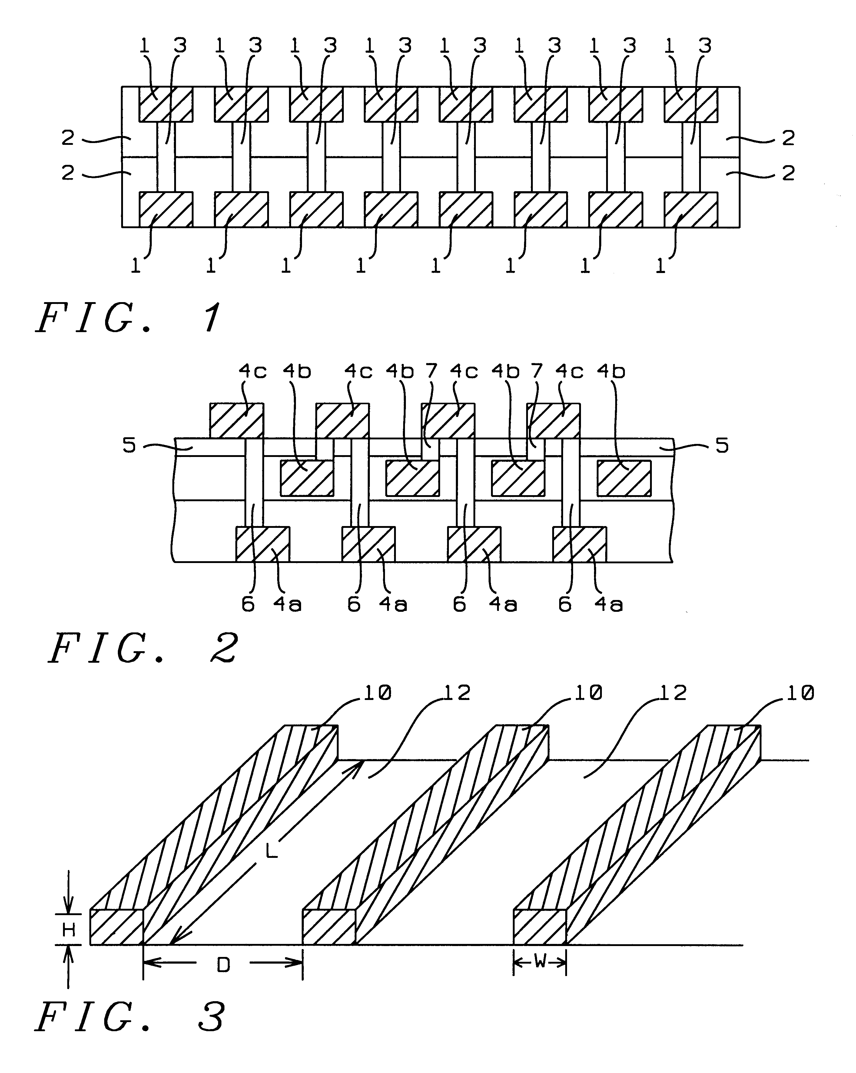
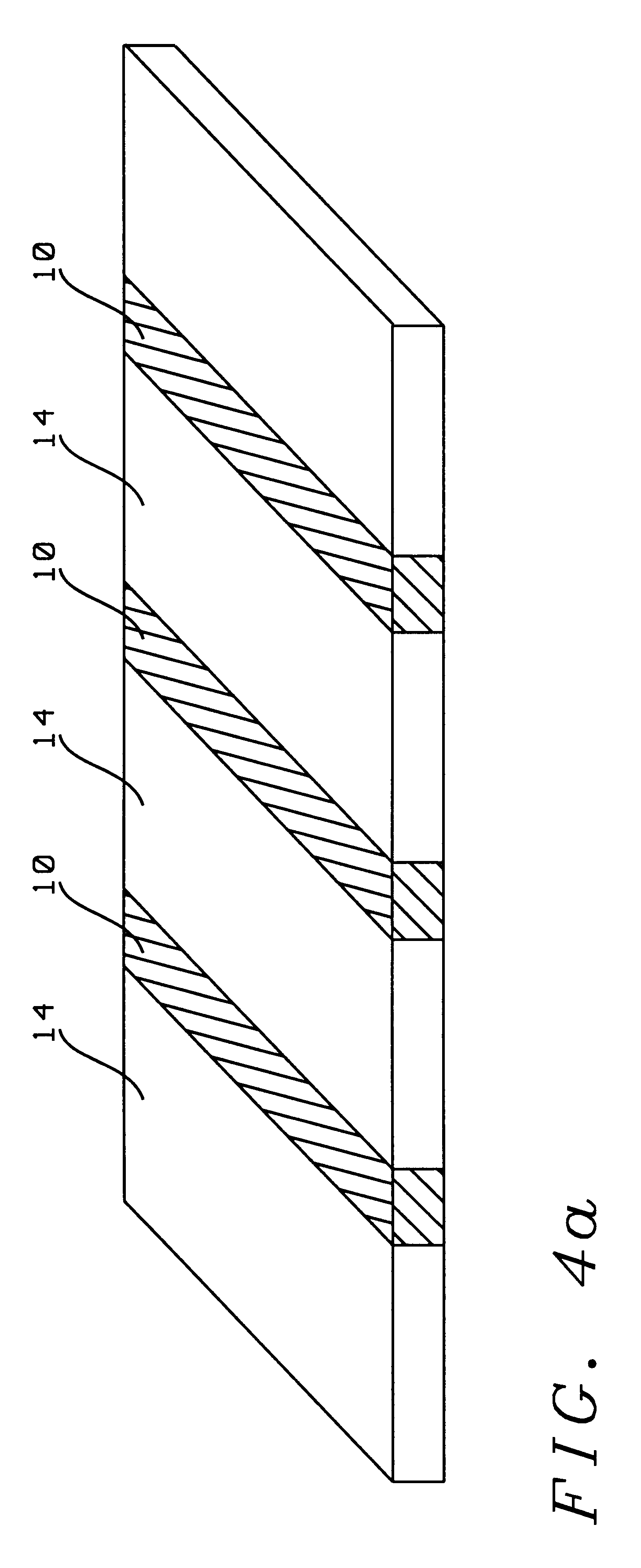
Referring first to FIG. 11, there is shown a schematic diagram of an alternative process to the steps provided in FIG. 3 and FIG. 4, wherein the metal segments of the first layer of the helical coil are now formed according to a copper damascene process. In this alternative process methodology, which is also in accord with the objects and methods of the present invention, a first IMD layer (15) of low-K dielectric material such as FSG, HSQ, MSQ, SILK or FLARE, is deposited to a thickness of be...


PUM


Abstract

A method for forming an RF inductor of helical shape having high Q and minimum area. The inductor is fabricated of metal or damascened linear segments formed on three levels of intermetal dielectric layers and interconnected by metal filled vias to form the complete helical shape with electrical continuity.

Description

1. Field of the InventionThis invention relates generally to the fabrication of integrated microelectronic circuitry having passive circuit components formed therein, more specifically to such a circuit having an inductor formed therein.2. Description of the Related ArtIt is well known that fabricating microelectronics circuitry, wherein active and passive components are monolthically integrated, is advantageous both from the standpoint of reducing manufacturing costs and from the standpoint of producing a circuit with improved operating characteristics. When considering methods of forming such passive components, however, inductors pose more challenges than either resistors or capacitors. For the purposes that they are required, microelectronic inductors must have both a high inductance (eg. to reduce power consumption) and high quality factor (Q factor.) Quality factor is defined as the ratio of energy stored to energy dissipated (Es / Ed) by a device, which can be shown to be equal...

Claims


Application Information

Patent Timeline
IPC IPC(8): H01L21/02H01L23/52H01L23/522H01L27/08
CPCH01L23/5227H01L28/10H01L27/08H01L2924/3011H01L2924/0002H01L2924/00
Inventor CHA, RANDALLLEE, TAE JONGSEE, ALEXCHAN, LAPTEE, CHUA CHEE
Owner CHARTERED SEMICONDUCTOR MANUFACTURING
Why Eureka
Try Eureka