Multiple threshold voltage FET using multiple work-function gate materials

a gate material and work function technology, applied in the field of electrical semiconductor devices and methods of fabrication, can solve the problems of gate control finite depth, threshold voltage, v.sub.t, and significant disadvantage of fet,

Inactive Publication Date: 2002-09-10
GLOBALFOUNDRIES INC
View PDF11 Cites 36 Cited by
  • Summary
  • Abstract
  • Description
  • Claims
  • Application Information

AI Technical Summary

Benefits of technology

In a second aspect, the present invention is directed to an integrated circuit chip having a plurality of field effect transistors therein, the transistors having narrow channel thickness and different threshold voltages, the threshold voltages determined by combination and adjacent positioning of at least two different gate materials, wherein the gate materials represent at least two different work functions.
At least two different work functions are averaged to form one total work function for one of the plurality of field effect tran

Problems solved by technology

Generally, a FET has a significant disadvantage in that the threshold voltage, V.sub.T, usually varies with respect to geometry, the channel length L, and the drain bias.
As gate lengths scale below 50 nm, FET scaling becomes limited by the finite depth of the gate control.
As the channel length, L, decreases, there is a considerable problem with a diminishing threshold voltage, V.sub.T.
This effect severely impairs device performance and makes it difficult to design integrated circuits with short channel lengths.
This problem with threshold voltage control is not apparent until the channel length approaches submicron levels.
However, dopant diffusion from a gate electrode into an un

Method used


Image

  • Multiple threshold voltage FET using multiple work-function gate materials
  • Multiple threshold voltage FET using multiple work-function gate materials
  • Multiple threshold voltage FET using multiple work-function gate materials

Examples


Embodiment Construction

)

In describing the preferred embodiment of the present invention, reference will be made herein to FIGS. 1-11 of the drawings in which like numerals refer to like features of the invention. Features of the invention are not necessarily shown to scale in the drawings.

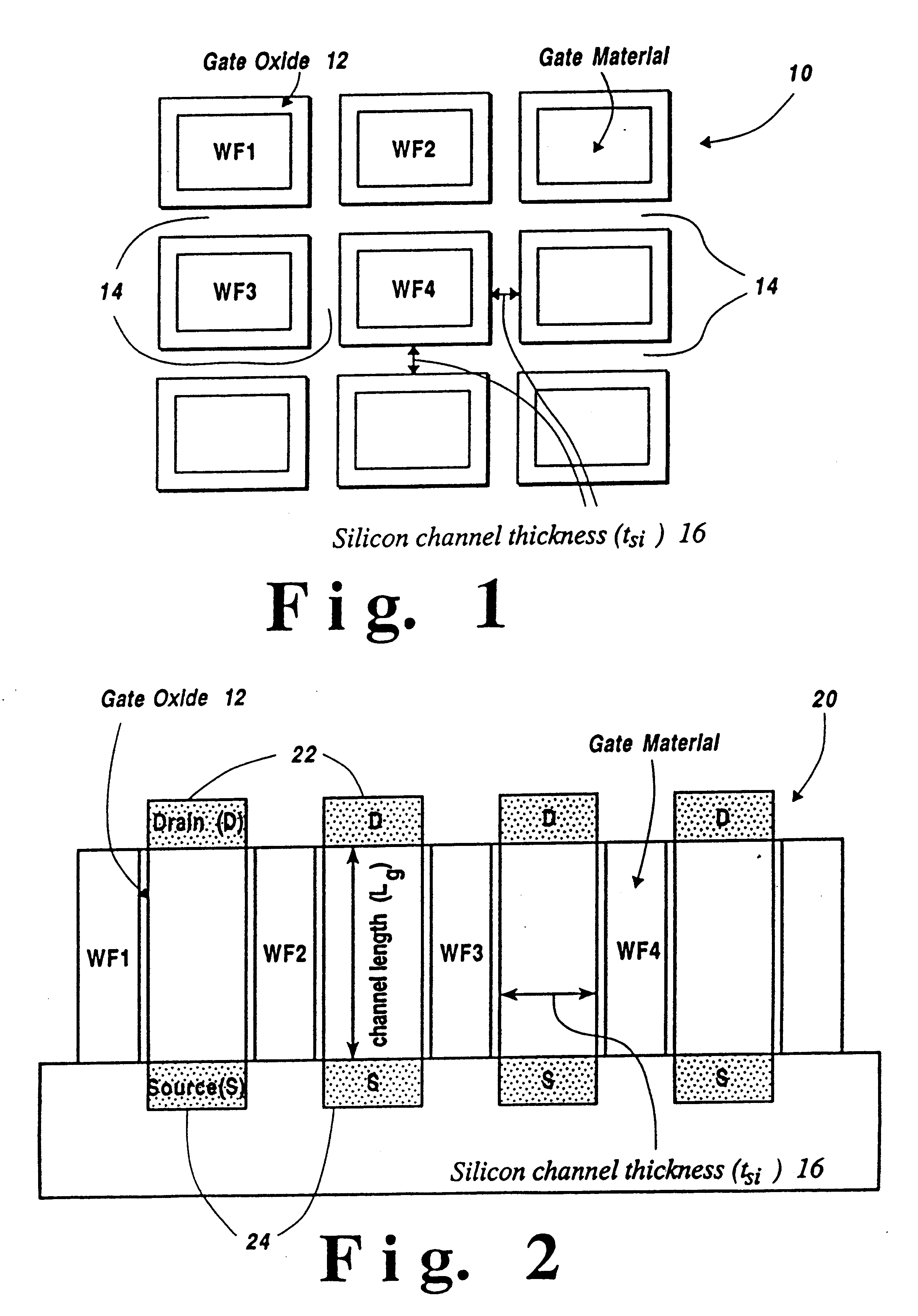
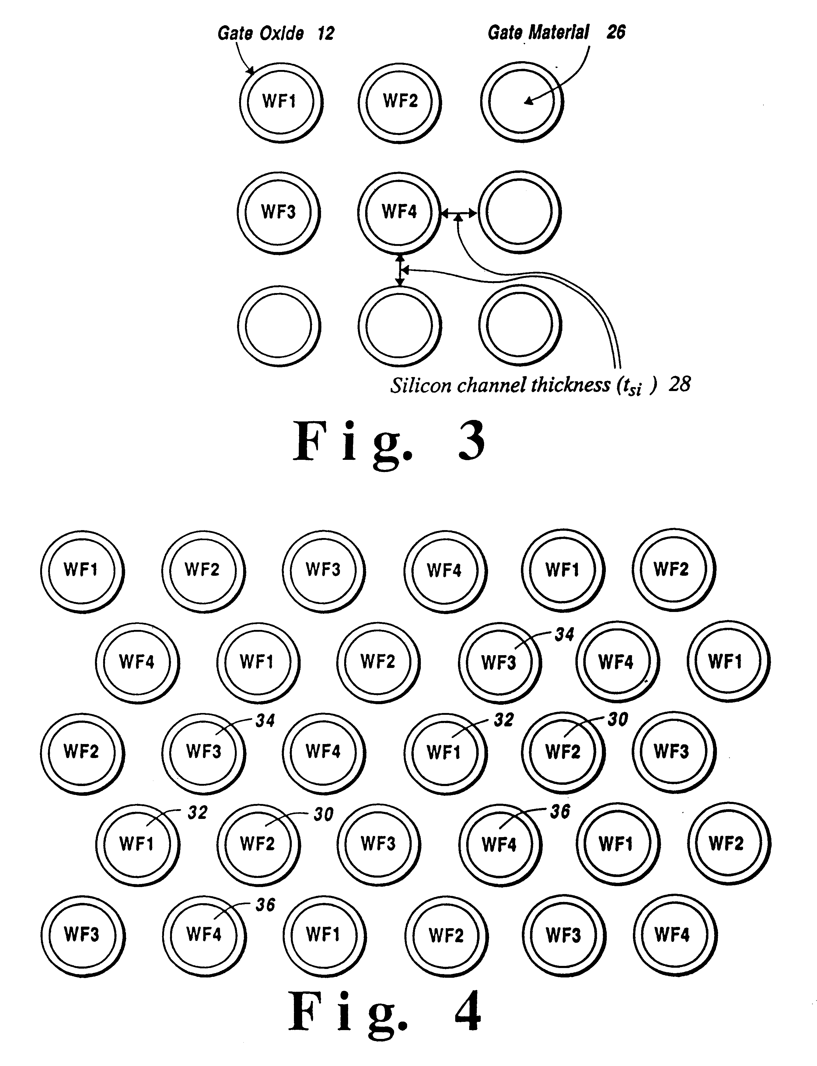
The threshold voltage of a field effect transistor with a very thin silicon channel and surrounded by gate materials on, for example, four sides of a square, would be the threshold voltage due to the average of the work function of the gate materials on the four sides. The gate materials may be, for example, n.sup.+ polysilicon gate, p.sup.+ polysilicon gate, tungsten, TiN, and the like.

FIG. 1 illustrates a top level view of FET 10 of the instant invention, having a square gate and rectangular channel. Gate oxide 12 surrounds different types of gate material with work functions WF1-WF4, respectively. The channel thickness of the silicon 16, t.sub.si, is the linear distance between each gate oxide layers surrounding each ...


PUM


Abstract

A shorter gate length FET for very large scale integrated circuit chips is achieved by providing a wafer with multiple threshold voltages. Multiple threshold voltages are developed by combining multiple work function gate materials. The gate materials are geometrically aligned in a predetermined pattern so that each gate material is adjacent to other gate materials. A patterned linear array embodiment is developed for a multiple threshold voltage design. The method of forming a multiple threshold voltage FET requires disposing different gate materials in aligned trenches within a semiconductor wafer, wherein each gate material represents a separate work function. The gate materials are arranged to be in close proximity to one another to accommodate small gate length designs.

Description

1. Field of the InventionThe present invention relates to an electronic semiconductor device and method of fabrication, particularly to voltage threshold adjustment for field effect transistors (FETs), and more particularly to the combination of geometry and multiple gate materials used to establish a total work function for a predetermined threshold voltage during gate fabrication.2. Description of Related ArtThe voltage threshold for a field effect transistor, for example a metal-oxide-semiconductor (MOSFET), is the gate voltage necessary to initiate conduction. Generally, a FET has a significant disadvantage in that the threshold voltage, V.sub.T, usually varies with respect to geometry, the channel length L, and the drain bias. In a polysilicon gate FET, the type of doping in the polysilicon of the gate electrode has a large influence on the threshold voltage. The polysilicon is typically heavily doped to achieve low resistivity. The Fermi energy of heavily doped (n-type) polysi...

Claims


Application Information

Patent Timeline
IPC IPC(8): H01L21/70H01L21/8234
CPCH01L21/82345H01L29/4916H01L29/495H01L29/4966H01L29/66666H01L29/7827H01L29/4238
Inventor ADKISSON, JAMES W.BALLANTINE, ARNE W.DIVAKARUNI, RAMACHANDRAJOHNSON, JEFFREY B.JONES, ERIN C.WONG, HON-SUM P.
Owner GLOBALFOUNDRIES INC
Why Eureka
Try Eureka