Patterning microelectronic features without using photoresists

a microelectronic feature and photoresist technology, applied in the field of integrated circuit storage devices, can solve the problems of requiring many more processing steps, requiring multiple metalization deposition steps, and complex processes,

Inactive Publication Date: 2002-09-17
IBM CORP
View PDF6 Cites 10 Cited by
  • Summary
  • Abstract
  • Description
  • Claims
  • Application Information

AI Technical Summary

Problems solved by technology

These processes are rather complex and require many more processing steps to complete.
The prior art damascene process has the disadvantag

Method used


Image

  • Patterning microelectronic features without using photoresists
  • Patterning microelectronic features without using photoresists
  • Patterning microelectronic features without using photoresists

Examples


Embodiment Construction

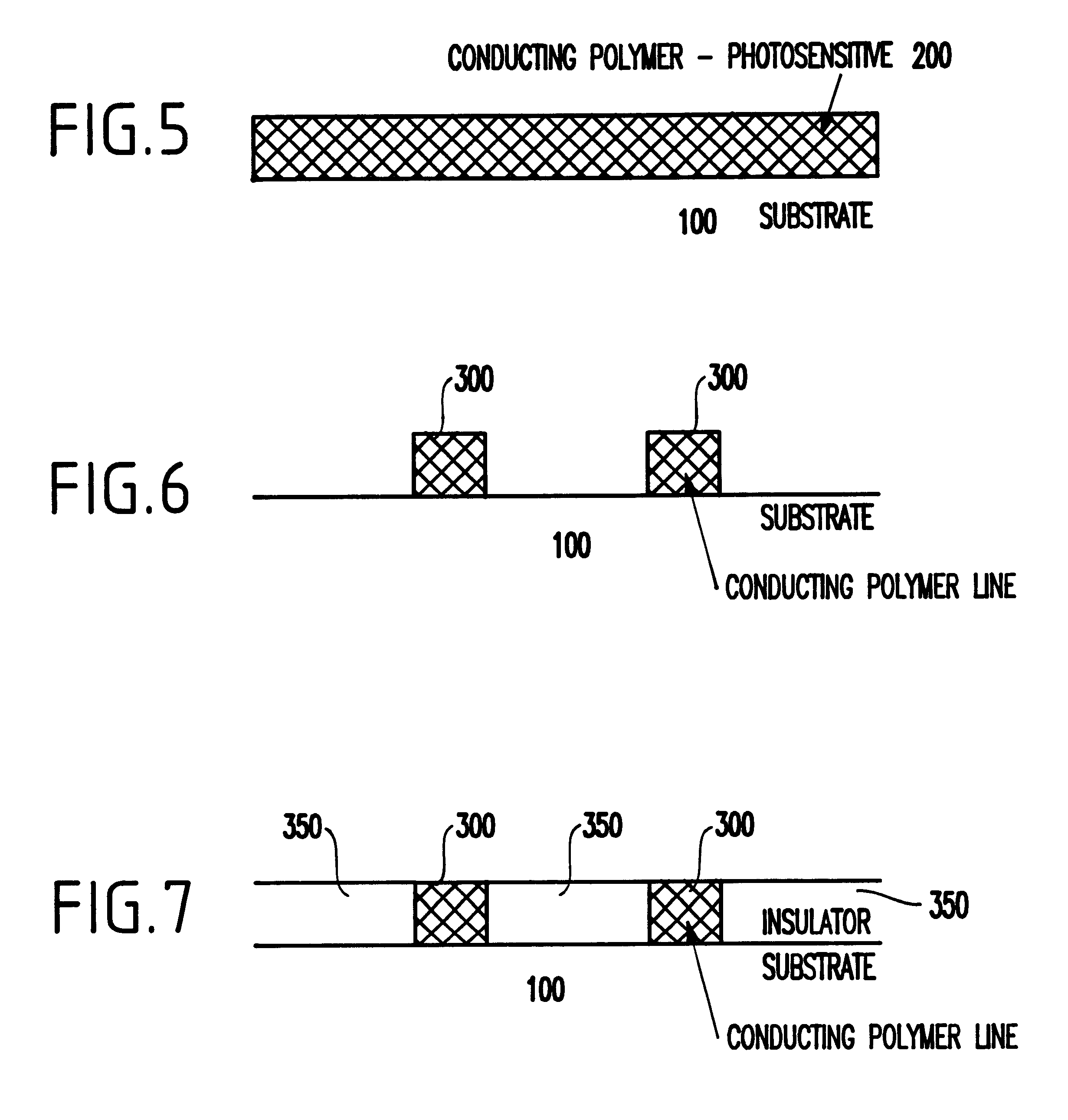
As mentioned above, there is a need to simply the processing steps in a traditional damascene process. The invention addresses this need by providing a simplified approach for producing micron and sub micron metallic conducting lines embedded in an insulating dielectric layer. In a preferred embodiment, an alternative methodology to the "damascene" approach which is being referred to as the "cloisonne" or "inverse damascene" approach is disclosed.

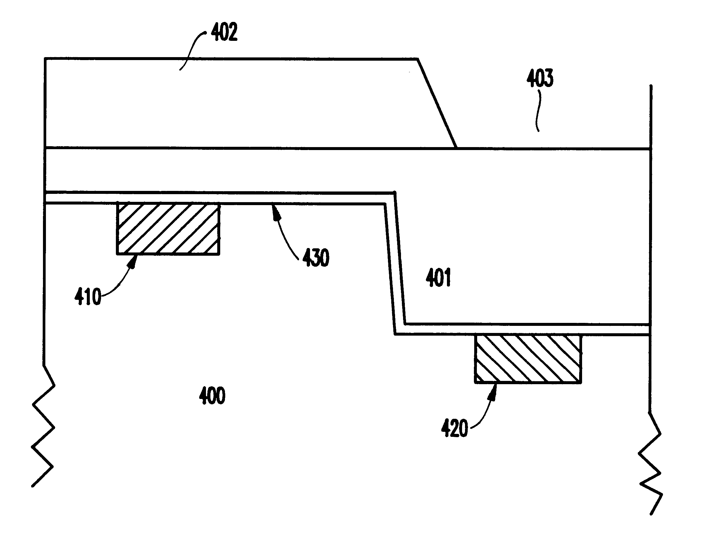
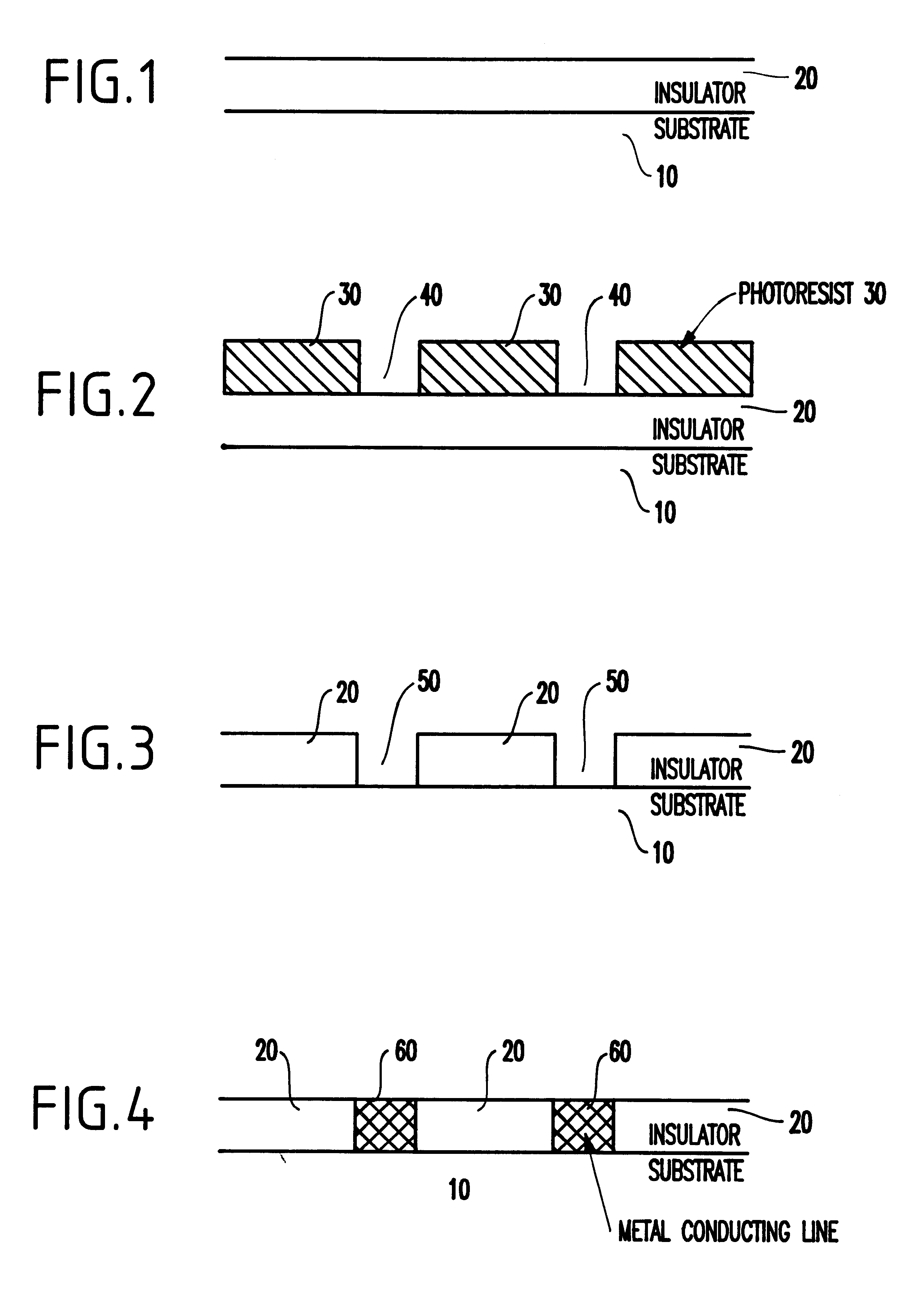
Referring now to the drawings, and more particularly to FIGS. 1 through 4, there are shown the conventional embodiments of the damascene method and structure. The prior art method of producing conducting lines embedded in an insulating matrix is called the damascene process. The prior art damascene process has the disadvantage of requiring etching of the insulating layer and / or requiring multiple metalization deposition steps contrary to the current disclosure. With the traditional damascene process, a thin film insulator 20 is first deposi...


PUM

PropertyMeasurementUnit
Electrical conductoraaaaaaaaaa
Metallic bondaaaaaaaaaa
Photosensitivityaaaaaaaaaa

Abstract

A method and structure for producing metallic polymer conductor lines comprising of an alternative methodology to a traditional damascene approach, called a cloisonne or inverse damascene approach. The cloisonne approach comprises the steps of coating a photosensitive polymer such as pyrrole or aniline with a silver salt on a semiconductor substrate. Using standard photolithography and resist developing techniques, the conducting polymer is exposed to a wet chemical developer, removing a portion of the exposed conducting polymer region, leaving only conducting polymer lines on top of the substrate. Next, an insulating dielectric layer is deposited over the entire structure and a chemical mechanical polish planarization of the insulator is performed creating the conducting polymer lines. Included in another aspect of the invention is a method and structure for a self-planarizing interconnect material comprising a conductive polymer thereby reducing the number of processing steps relative to the prior art.

Description

1. Field of the InventionThe present invention generally relates to integrated circuit storage devices and more particularly to an improved method for producing electrically conductive embedded lines in an insulating dielectric layer.2. Description of the Related ArtAn integrated circuit, or any other semiconductor device is constructed to have several electronic circuit elements interwoven on a single body of semiconductor material. The various circuit elements, such as amplifiers, conductors, diodes, resistors, and transistors, to name a few, are integrated through conductive connectors to form a complete circuit which can contain millions of individual circuit elements. Technological advances in semiconductor material selection and other processing techniques have resulted in allowing for an increased number of individual circuit elements on a single semiconductor body, while reducing the overall size of the individual circuit elements. This reduction in overall size yields a red...

Claims


Application Information

Patent Timeline
IPC IPC(8): H01L21/70H01L21/768H01L21/288H01L21/02H01L21/3213H05K3/02H01B13/00G03F7/40H01L21/3205H01L23/52
CPCH01L21/288H01L21/32134H05K3/02H01L21/76885Y10T29/49155Y10T29/49156
Inventor CLEVENGER, LAWRENCE A.HSU, LOUIS L.RADENS, CARL J.WANG, LI-KONGWONG, KEITH KWONG HON
Owner IBM CORP
Why Eureka
Try Eureka