

Interconnect structure for stacked semiconductor device
a technology of interconnection structure and semiconductor, which is applied in the direction of solid-state devices, basic electric elements, manufacturing tools, etc., can solve the problems of loss of planar smoothness, the surface of multi-layer films becomes increasingly irregular, and the above-mentioned structure cannot be directly used
- Summary
- Abstract
- Description
- Claims
- Application Information
AI Technical Summary
Benefits of technology
Problems solved by technology
Method used
Image

Examples
example 2
Specified Example 2 of the Manufacturing Process
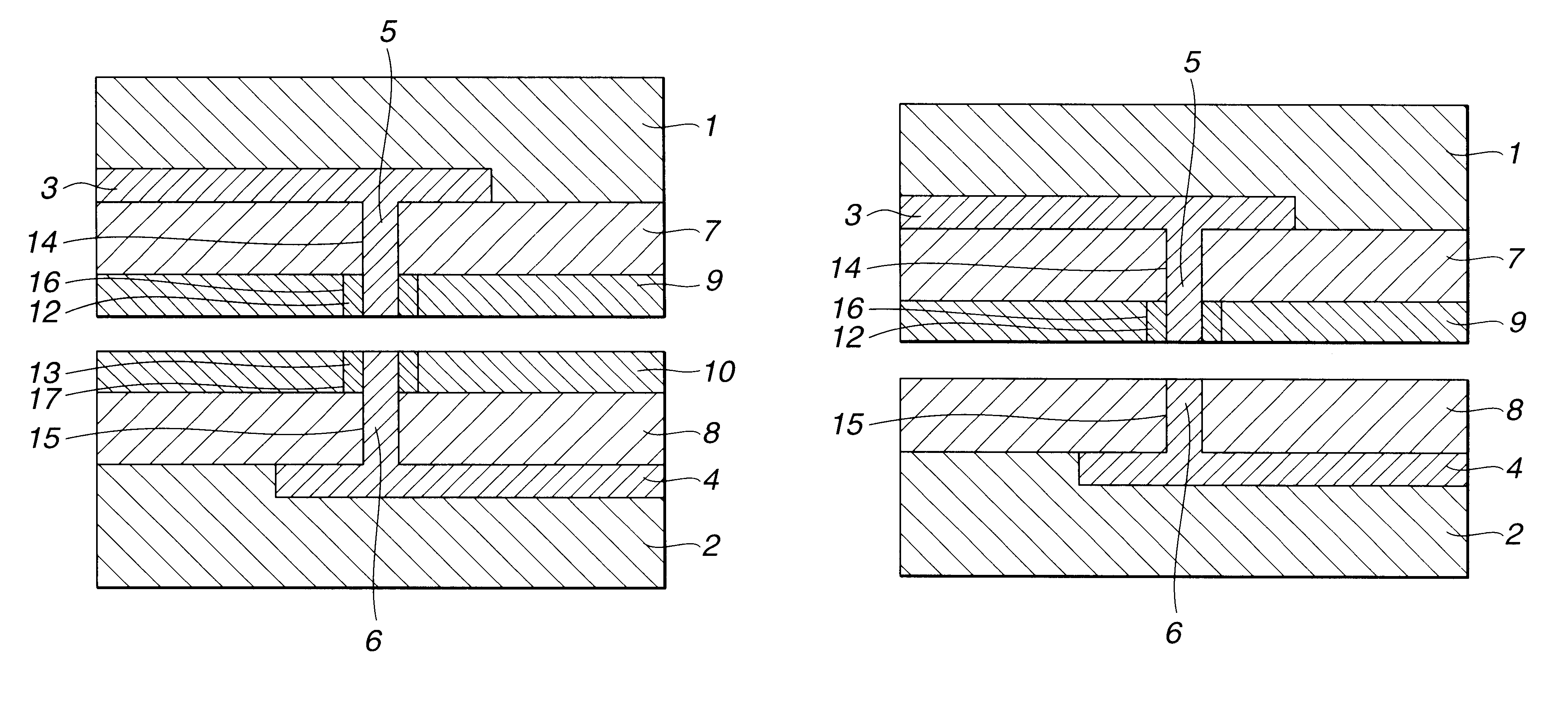
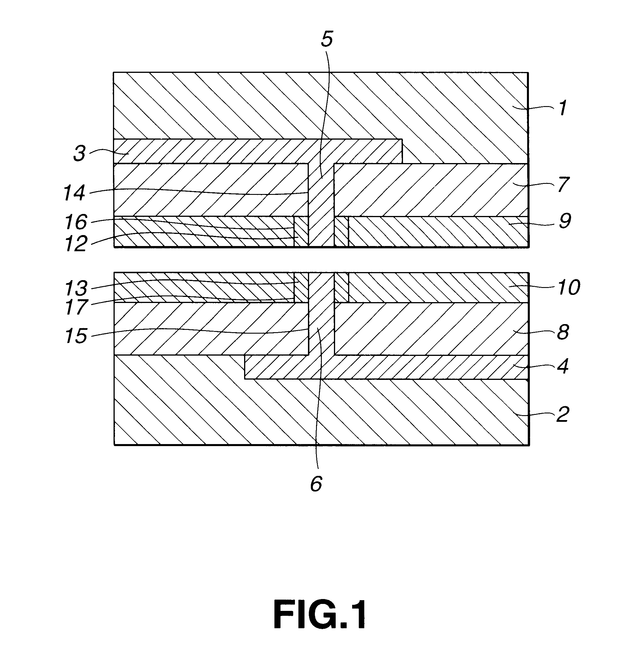
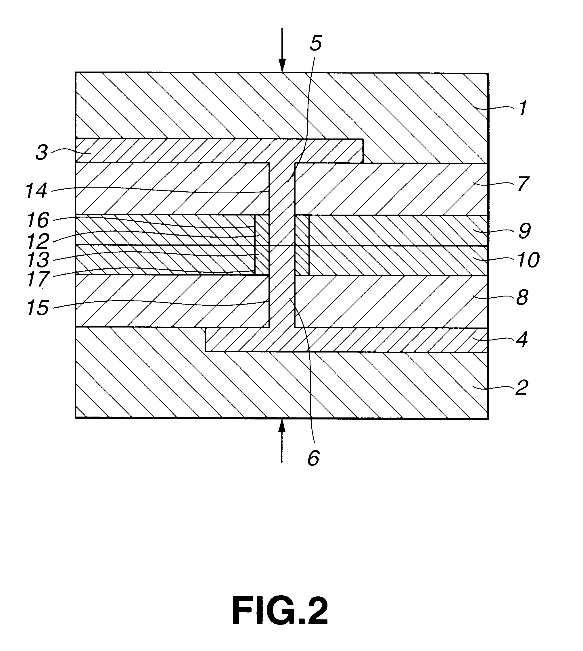
In the present embodiment, two semiconductor substrates, each carrying semiconductor elements, are connected to each other by the following process steps:
(1) a step of previously providing a wiring electrode on a first semiconductor substrate;
(2) a step of sequentially depositing an insulating layer and a grounding layer on the first substrate and boring through-holes connecting to the wiring electrode in the insulating layer and the grounding layer;
(3) a step of forming a through-hole wiring in the through-holes for electrical connection to the wiring electrode;
(4) a step of forming an insulator between in the through-hole wiring the through-hole in the grounding layer and the grounding layer;
(5) a step of smoothing the major surface of the first substrate;
(6) a step of previously providing a wiring electrode on a second semiconductor substrate;
(7) a step of depositing an insulating layer on the second semiconductor substrate and form...
example 3
Specified Example 3 of the Manufacturing Process
In the present embodiment, two semiconductor substrates, each carrying semiconductor element, are connected to each other by the following process steps:
(1) a step of previously taking out a wiring electrode on a first semiconductor substrate;
(2) a step of sequentially depositing an insulating layer, a grounding layer and another insulating layer on the first substrate and boring through-holes connecting to the wiring electrode in the insulating layer, grounding layer and the other insulating layer;
(3) a step of forming a through-hole wiring in the through-holes for electrical connection to the wiring electrode;
(4) a step of forming an insulator between the through-hole wiring in the through-holes in the grounding layer and the grounding layer;
(5) a step of smoothing the major surface of the first substrate;
(6) a step of previously taking out a wiring electrode on a second semiconductor substrate;
(7) a step of sequentially depositing a...
example 4
Specified Example 4 of the Manufacturing Process
In the present embodiment, two semiconductor substrates, each carrying semiconductor elements, are connected to each other by the following process steps:
(1) a step of taking out a wiring electrode and a grounding electrode on a first substrate;
(2) sequentially depositing an insulating layer and a grounding layer on a first substrate and forming a through-hole connecting to the grounding electrode in the insulating layer;
(3) forming a through-hole grounding wiring electrically connecting to the grounding electrode in the through-hole;
(4) smoothing the surface of the first substrate;
(5) previously taking out a grounding electrode on a second semiconductor substrate;
(6) sequentially depositing an insulating layer and a grounding layer on the second substrate and forming a through-hole connecting to the grounding electrode in the insulating layer;
(7) forming a through-hole grounding wiring electrically connecting to the grounding electrod...
PUM
| Property | Measurement | Unit |
|---|---|---|
| electrically conductive | aaaaa | aaaaa |
| semiconductor | aaaaa | aaaaa |
| inner diameter | aaaaa | aaaaa |
Abstract
Description
Claims
Application Information