Three dimensional optical beam induced current (3-D-OBIC)

Inactive Publication Date: 2002-10-15
CARL ZEISS JENA GMBH
View PDF16 Cites 18 Cited by
  • Summary
  • Abstract
  • Description
  • Claims
  • Application Information

AI Technical Summary

Benefits of technology

It is an object to provide a multiphoton laser scanning microscopy in material analysis, especially in the analysis of structured silicon wafers by means of non-optical detection techniques such as, e.g., OBIC or LIVA. In accordance with the invention, the high localization of the multiphoton excitation in all three spatial coordinates through the use of high-aperture microscope objectives enables nondestructive three-dimensional localization

Problems solved by technology

The disadvantage of this method is that generating

Method used


Image

  • Three dimensional optical beam induced current (3-D-OBIC)
  • Three dimensional optical beam induced current (3-D-OBIC)
  • Three dimensional optical beam induced current (3-D-OBIC)

Examples


Embodiment Construction

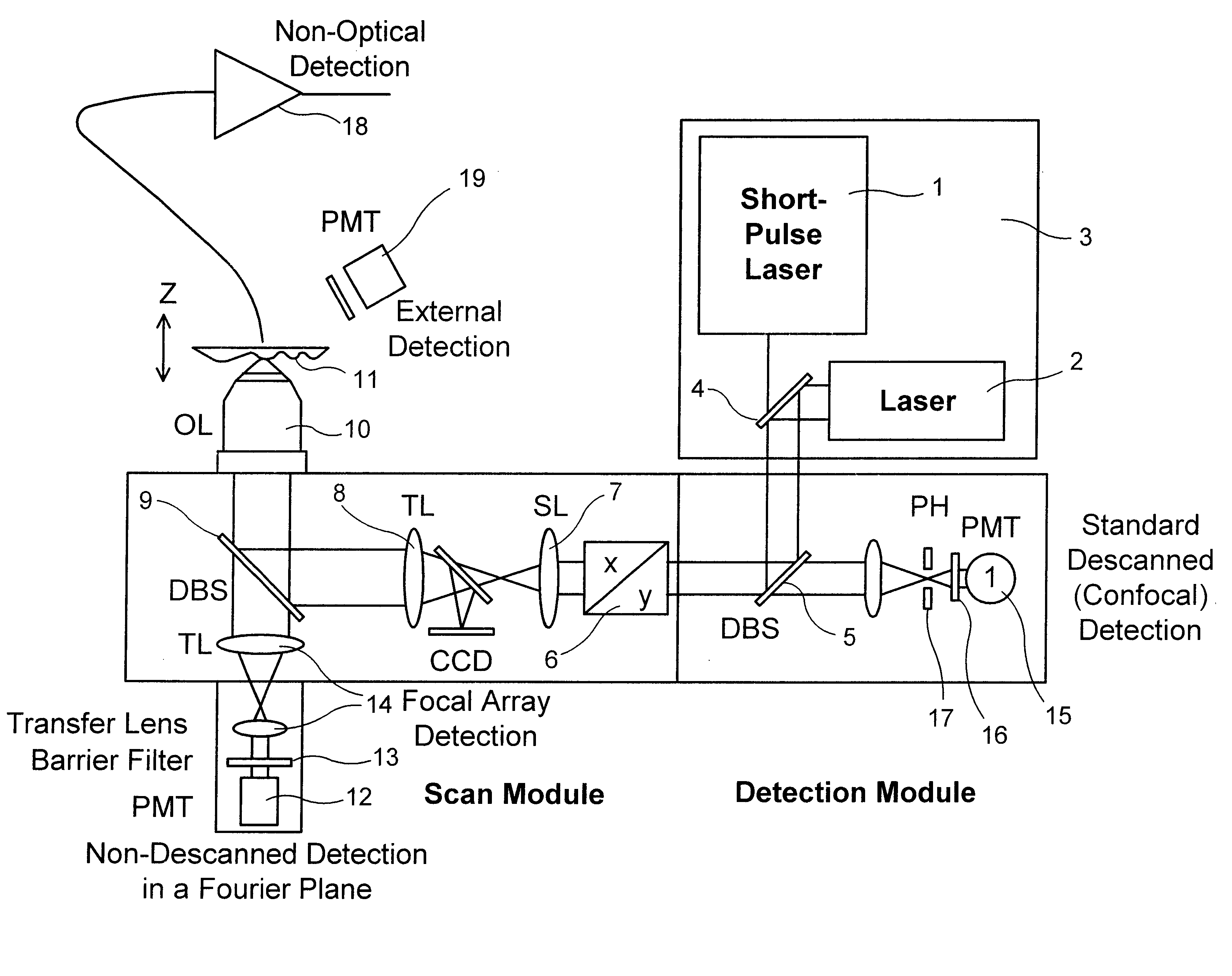
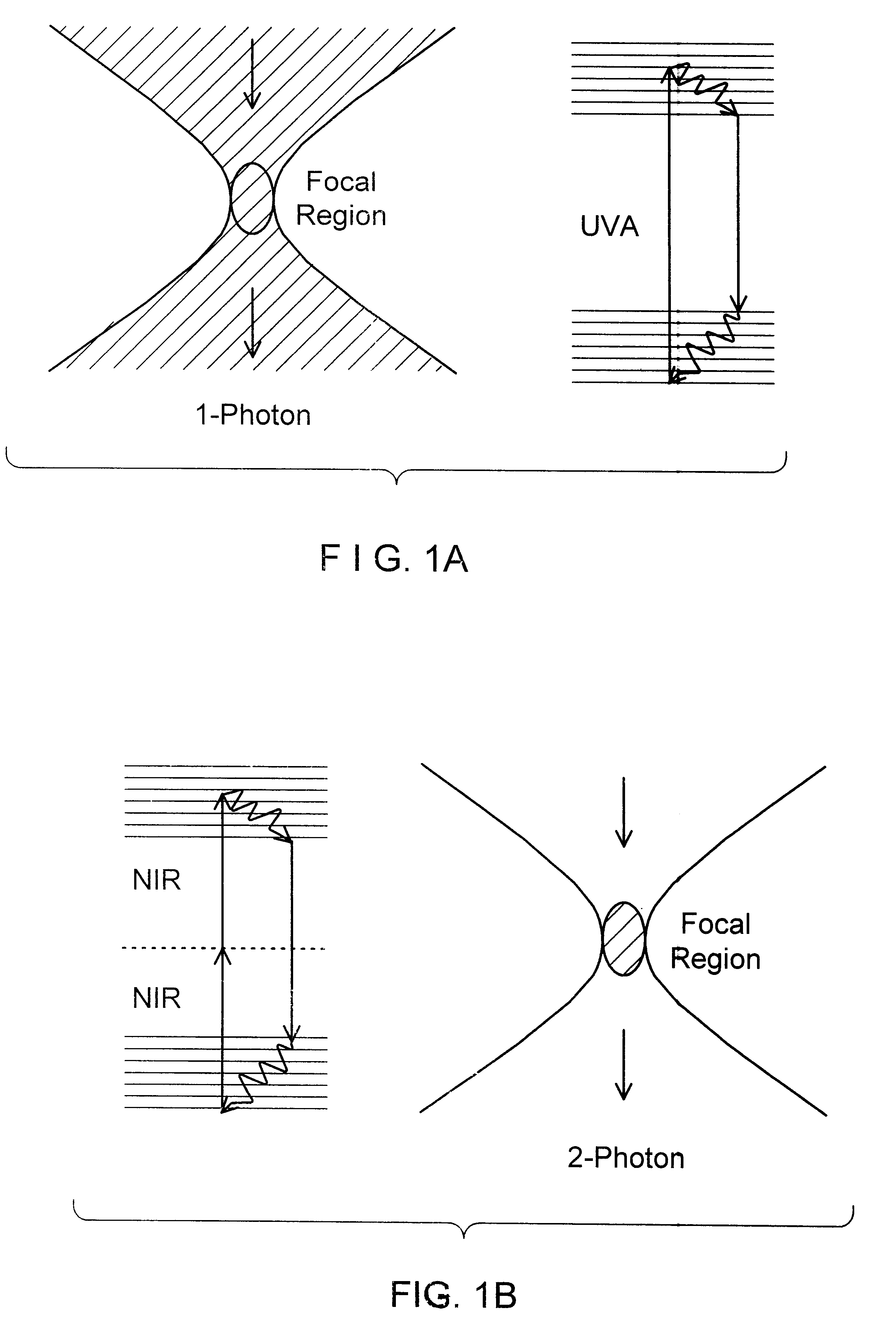
FIG. 1a shows the propagation of the laser beam which is focussed by means of a high-aperture microscope objective. In the case of single-photon excitation, excitation results along the entire laser beam cone. However, by using a confocal aperture, the light coming from the focus can be discriminated relative to the extra-focal light.

FIG. 1b shows the propagation of the laser beam focussed by means of a high-aperture microscope objective. In the case of two-photon excitation, [excitation] results only in the region of highest intensity, i.e., in the laser beam focus. This technique is accordingly also depth-discriminating without the use of a confocal aperture.

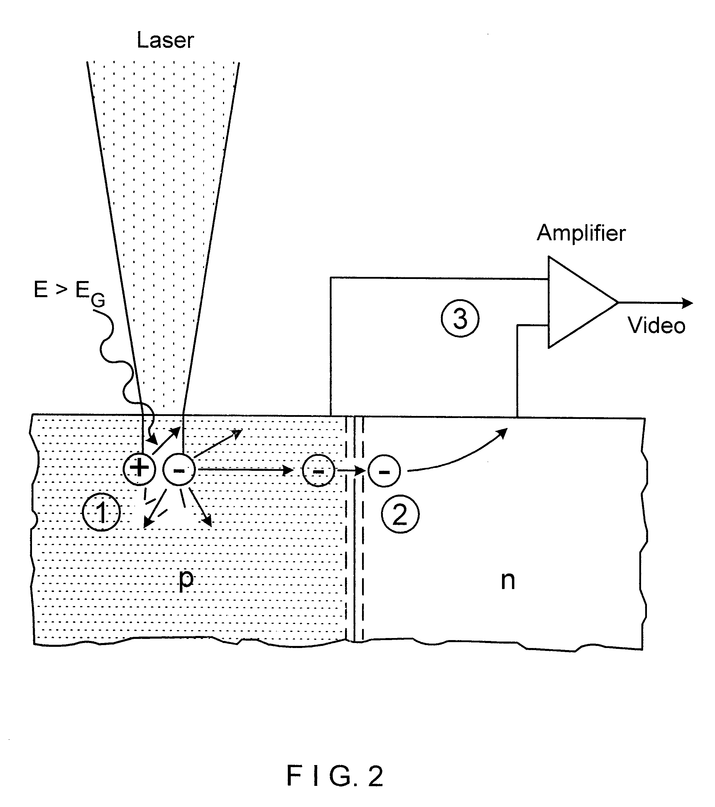
FIG. 2 If the band gap energy E.sub.G is less than the photon energy E of the incident light, electron hole pairs occur in a semiconductor (1). They recombine very quickly, in general, in the homogeneous semiconductor. When this takes place in the vicinity of a blocked p-n junction, the separation of the holes and electrons ta...


PUM


Abstract

The invention describes the use of multiphoton laser scanning microscopy in material analysis, especially in the analysis of structured silicon wafers by using non-optical detection techniques such as, e.g., OBIC (optical beam induced current) or LIVA (light induced voltage alteration). OBIC and LIVA make use of the generation of an electron-hole charge carrier current or a change in potential due to the scanning laser beam to localize lattice defects in crystalline materials, especially p-n junctions. By using the high localization of the multiphoton excitation in all three spatial coordinates using high-aperture microscope objectives in laser scanning microscopy, this technique enables nondestructive three-dimensional localization of crystal defects. Accordingly, this technique advantageously dispenses with the detection of lattice defects by using two-dimensional laser scanning microscopy and the subsequent required successive mechanical removal of the crystal structure in conjunction with electron microscopy for detecting the defects in the third dimension as well.

Description

In two-photon excitation (as a special case of multiphoton excitation), a transition is excited in the excitation structure (term diagram) of a gas, liquid or solid (such as electronic, vibrational or rotational transitions or fine structures) by means of the quasi-simultaneous absorption of two photons of the longer wavelengths .lambda..sub.1 and .lambda..sub.2 (where .lambda..sub.1 and .lambda..sub.2 can be identical or different), for which purpose an individual photon of the shorter wavelength (.lambda..sub.1 +.lambda..sub.2) / 4 would be necessary otherwise. Two photons in the "long wavelength" (e.g., in the red range) can thus, for example, excite a UV-absorbing transition which normally (i.e., in conventional single-photon excitation) absorbs in the short wavelength (e.g., in the blue range) (FIGS. 1a and 1b). Since two photons are needed to excite a two-photon transition, the transition rate for a given transition depends upon the square of the excitation intensity. For this r...

Claims


Application Information

Patent Timeline
IPC IPC(8): G02B21/00
CPCG02B21/002
Inventor SIMON, ULRICHDANZ, RAINERWOLLESCHENSKY, RALF
Owner CARL ZEISS JENA GMBH
Why Eureka
Try Eureka