Storage circuit with layered structure element

a technology of layered structure and storage circuit, which is applied in the direction of static storage, digital storage, instruments, etc., can solve the problems of problems to be solved, and inability to scale the thickness of oxide film in order to hold data, etc., to achieve low power consumption and low power consumption. , the effect of non-volatil

Inactive Publication Date: 2002-10-29
HITACHI LTD
View PDF3 Cites 20 Cited by
  • Summary
  • Abstract
  • Description
  • Claims
  • Application Information

AI Technical Summary

Benefits of technology

An object of the present invention is to solve the problems of the prior art, and to provide a storage circuit or a flip-flop circuit, which has low powe

Problems solved by technology

In future, when pursuing further minuteness, and when trying to achieve reduction of bit cost and high performance, there are problems to be solved in each of these aspects.
As regards further minuteness of the DRAM, a problem exists in measures for the structure of a capacity section, which results from the fact that the current DRAM adopts a cell structure of one transistor--one capacitor.
At present, the flash memory also has a problem of compatibility between minuteness and a life of a data storage period.
In addition, it is not possible to scale the thickness of the oxide film in order to hold data.
For these

Method used


Image

  • Storage circuit with layered structure element
  • Storage circuit with layered structure element
  • Storage circuit with layered structure element

Examples


Embodiment Construction

Before describing modes for carrying out the invention, general means according to the present invention will be listed and described as below.

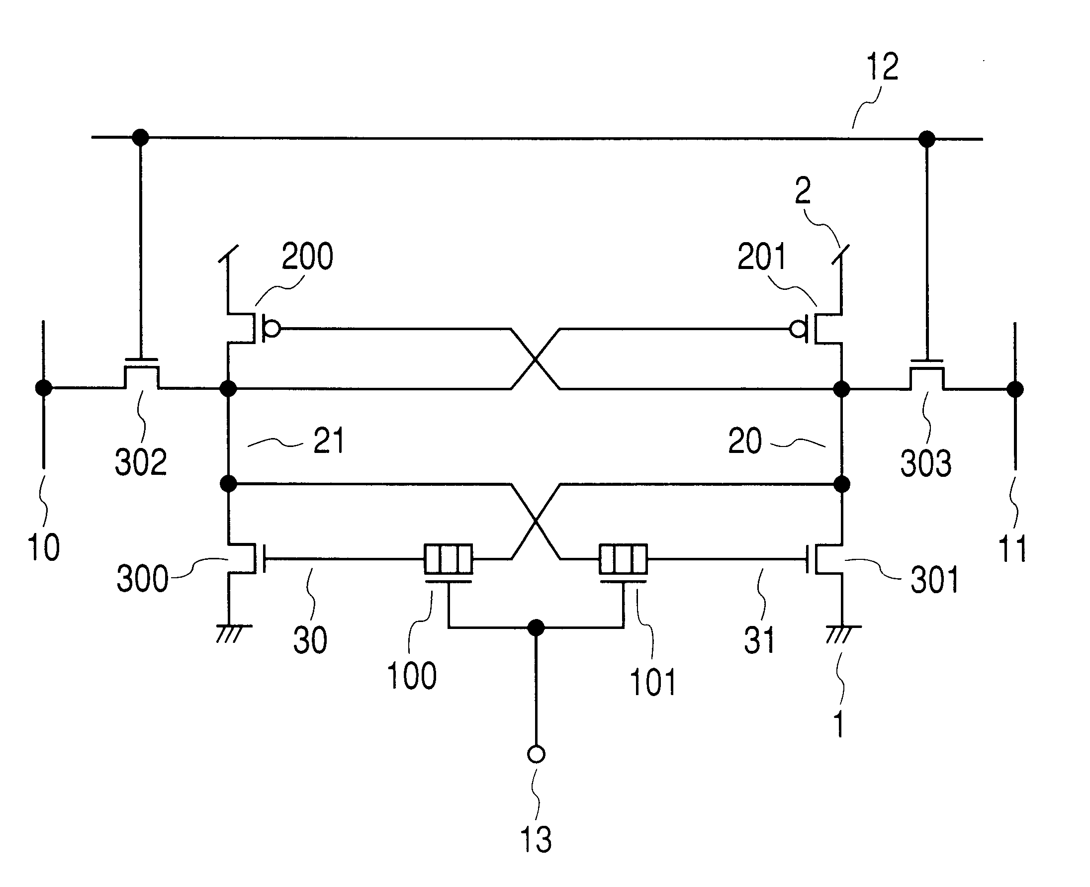
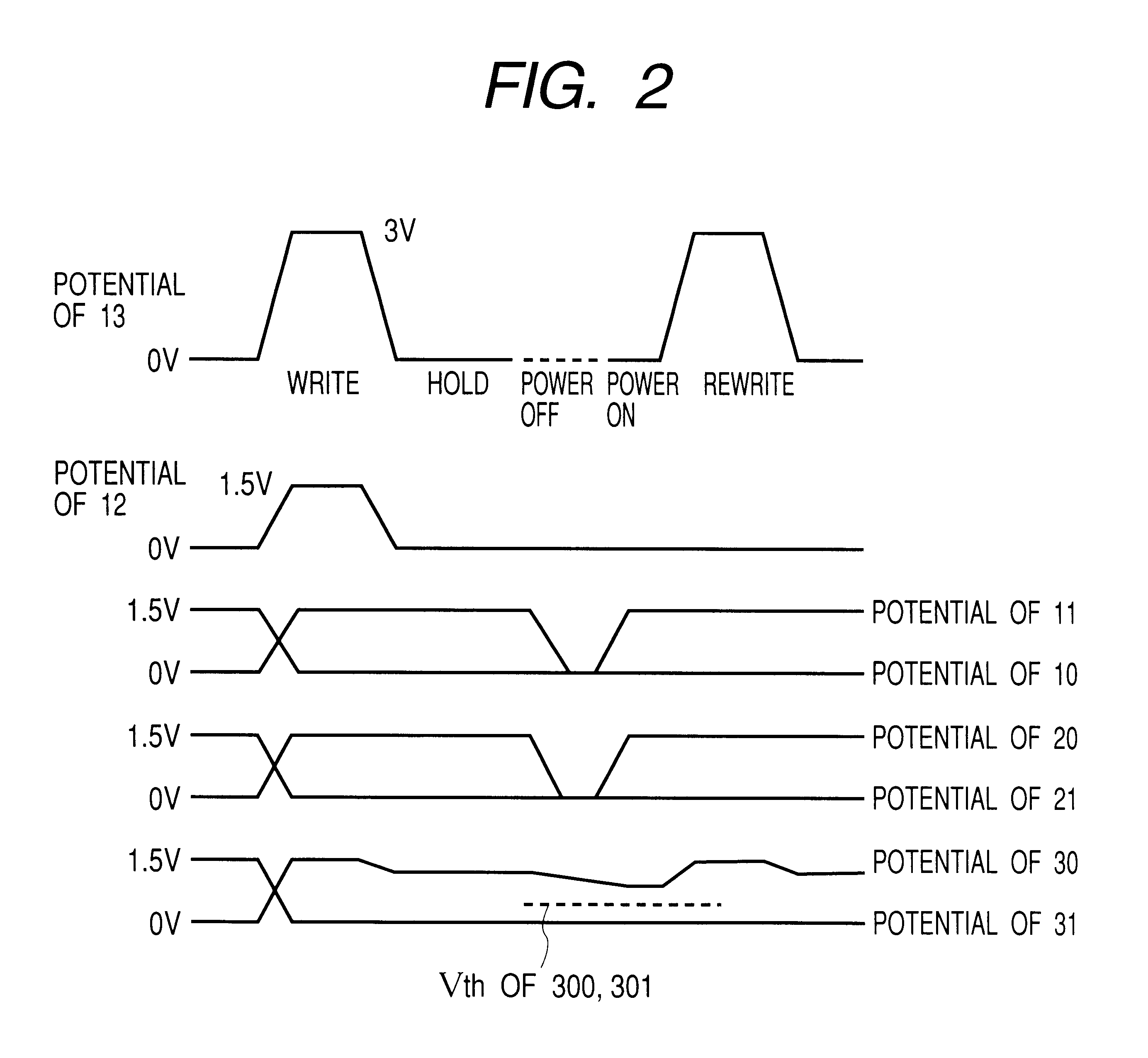
The present invention will be described with reference to FIGS. 1 and 2. FIG. 1 is a circuit diagram illustrating a flip-flop circuit according to the present invention. FIG. 2 is a time chart illustrating a waveform of operation when this circuit is used. FIG. 3 illustrates an example of memory device structure, which is used for the circuit.

An example of FIG. 1 shows a memory cell that uses a so-called flip-flop. In the so-called SRAM, a plurality of such memory cells is placed. In general, the plurality of memory cells is placed in a matrix form using data lines and word lines.

In FIG. 1, a reference numeral 1 is a negative power supply terminal (usually, GND); a reference numeral 2 is a positive power supply terminal (Vcc); reference numerals 10 and 11 are a write data line and a read data line respectively; a reference numeral 12 is a wri...


PUM


Abstract

The present invention provides a circuit, in which a device typified by a PLED element is built into a flip-flop. In this case, a storage node of the device is low leakage. According to the present invention, it is possible to realize a SRAM that has nonvolatility while achieving high-speed operation. It is also possible to realize a flip-flop having the same characteristics. An example of a typical mode of the present invention is a storage circuit characterized by the following: a storage element is a device incorporating: a first path for a carrier; a first mode for storing a charge that generates an electric field where conductivity of the first path is changed; and a barrier structure through which a second carrier moves in response to given voltage so that the second carrier is stored in the first node; and the storage circuit includes a second node, to which information stored in the first node is outputted steadily in a state in which power is supplied. The flip-flop and the SRAM are realized using such a basic circuit.

Description

The present invention relates to a storage circuit and a semiconductor memory device.At present, as typical large-capacity semiconductor memory devices, a DRAM (Dynamic Random Access Memory) and a flash memory are named. In future, when pursuing further minuteness, and when trying to achieve reduction of bit cost and high performance, there are problems to be solved in each of these aspects. As regards further minuteness of the DRAM, a problem exists in measures for the structure of a capacity section, which results from the fact that the current DRAM adopts a cell structure of one transistor--one capacitor. To be more specific, the problem relates to the measures for the so-called stacked structure, in which for example, a capacity section is laminated on a substrate.At present, the flash memory also has a problem of compatibility between minuteness and a life of a data storage period. Under the present circumstances, the flash memory is being developed with both of them as a backd...

Claims


Application Information

Patent Timeline
IPC IPC(8): G11C11/412G11C14/00G11C11/22
CPCG11C11/22G11C11/412G11C14/00Y10S257/903
Inventor TACHIBANA, SUGURUSASAKI, KATSUROITOH, KIYOOISHII, TOMOYUKI
Owner HITACHI LTD
Why Eureka
Try Eureka