Method of forming a semiconductor device having conductive bumps without using gold

a technology of conductive bumps and semiconductor devices, which is applied in the direction of semiconductor devices, basic electric elements, electrical equipment, etc., can solve the problems of high cost of high vacuum evaporator raw materials, high manufacturing cost of solder bumps, and high cost of operation and maintenance of high vacuum evaporators

Inactive Publication Date: 2002-12-03
NXP USA INC
View PDF10 Cites 107 Cited by
  • Summary
  • Abstract
  • Description
  • Claims
  • Application Information

AI Technical Summary

Problems solved by technology

One problem with conventional high-lead solder bumps is manufacturing cost.
High vacuum evaporators are expensive to purchase, operate, and maintain.
Raw materials used in the process are expensive.
One of the highest variable cost of the conventional C4 process is the gold evaporation process, particularly costs associated with the gold source itself.

Method used


Image

  • Method of forming a semiconductor device having conductive bumps without using gold
  • Method of forming a semiconductor device having conductive bumps without using gold
  • Method of forming a semiconductor device having conductive bumps without using gold

Examples


Embodiment Construction

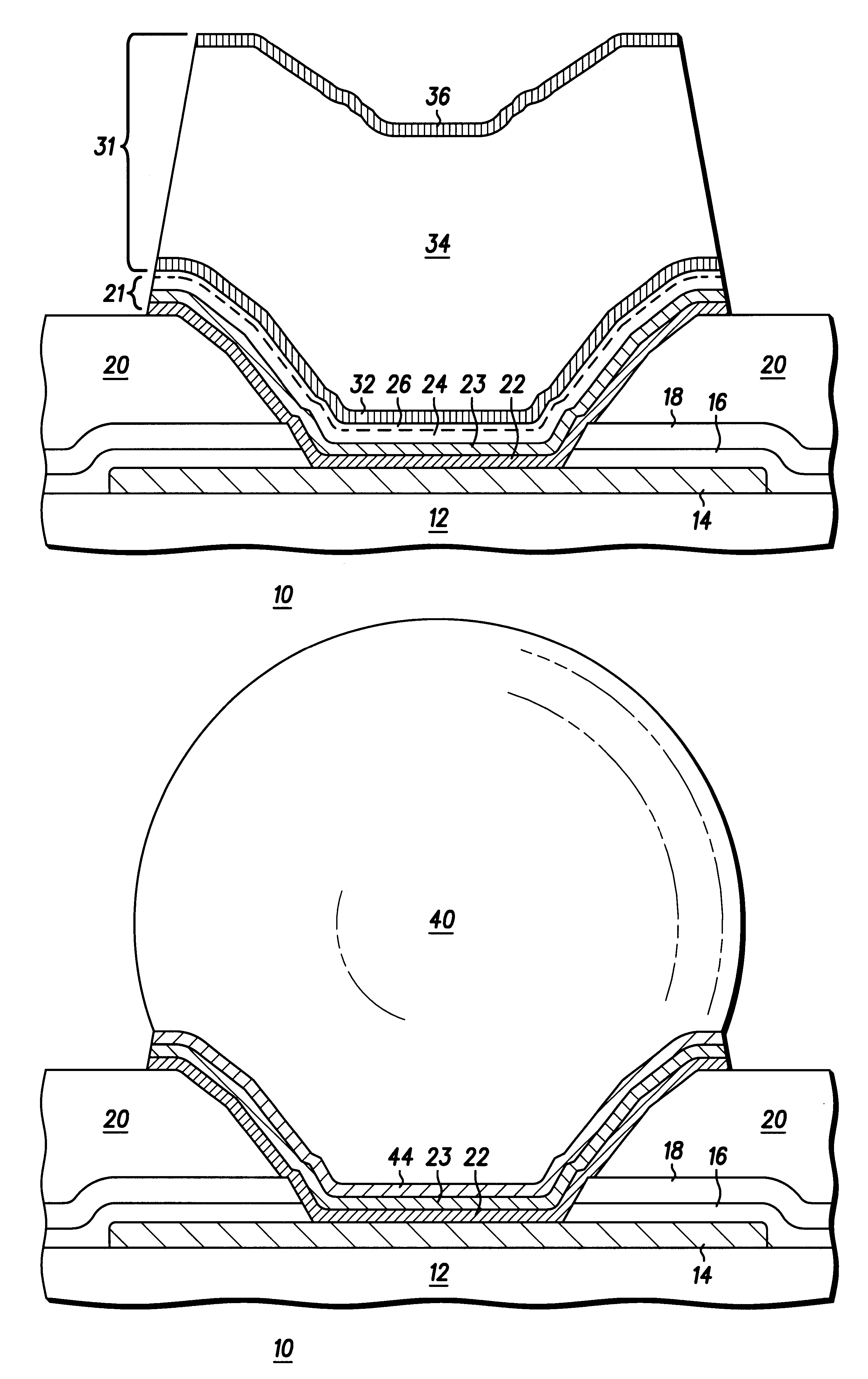
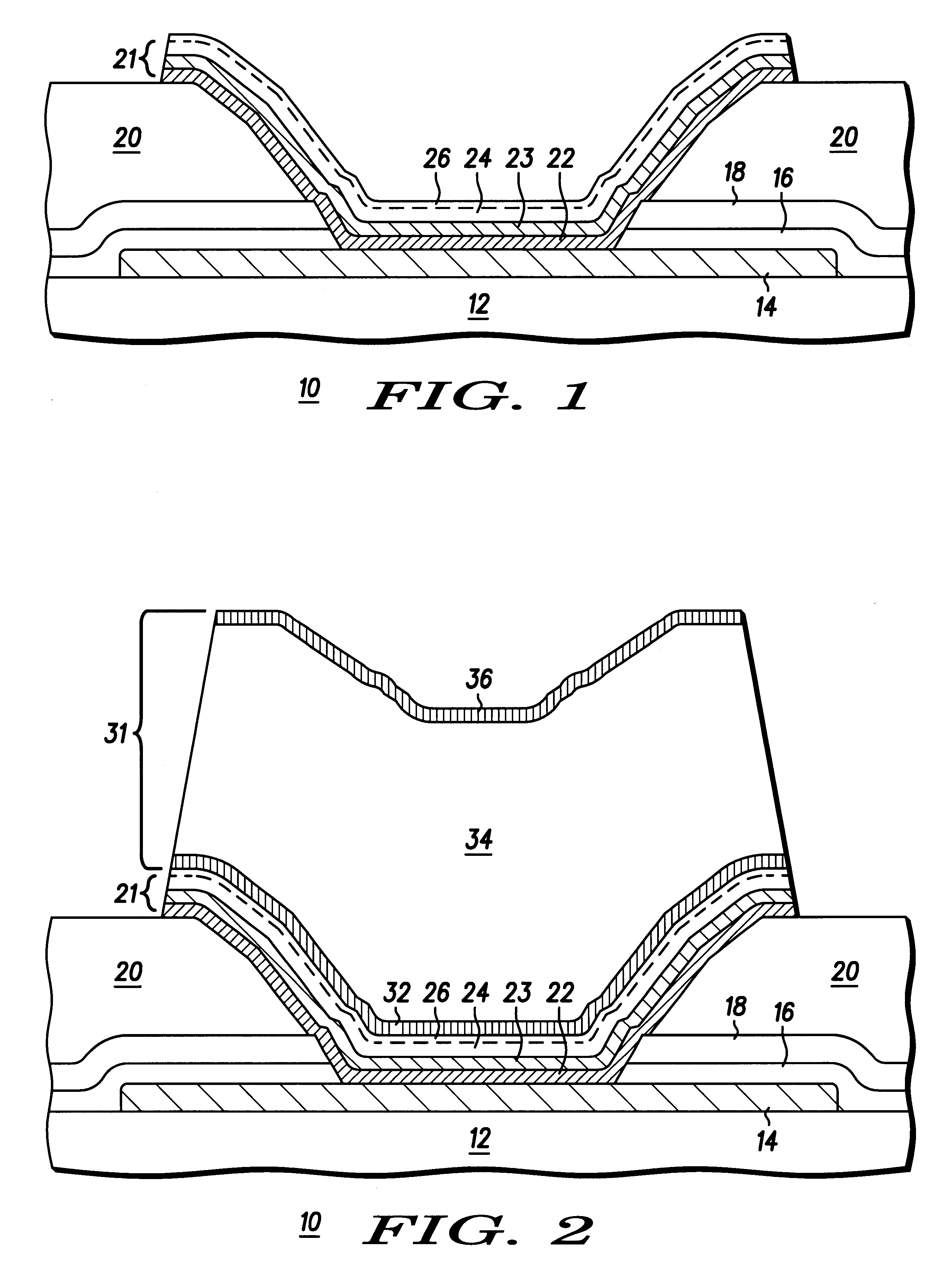
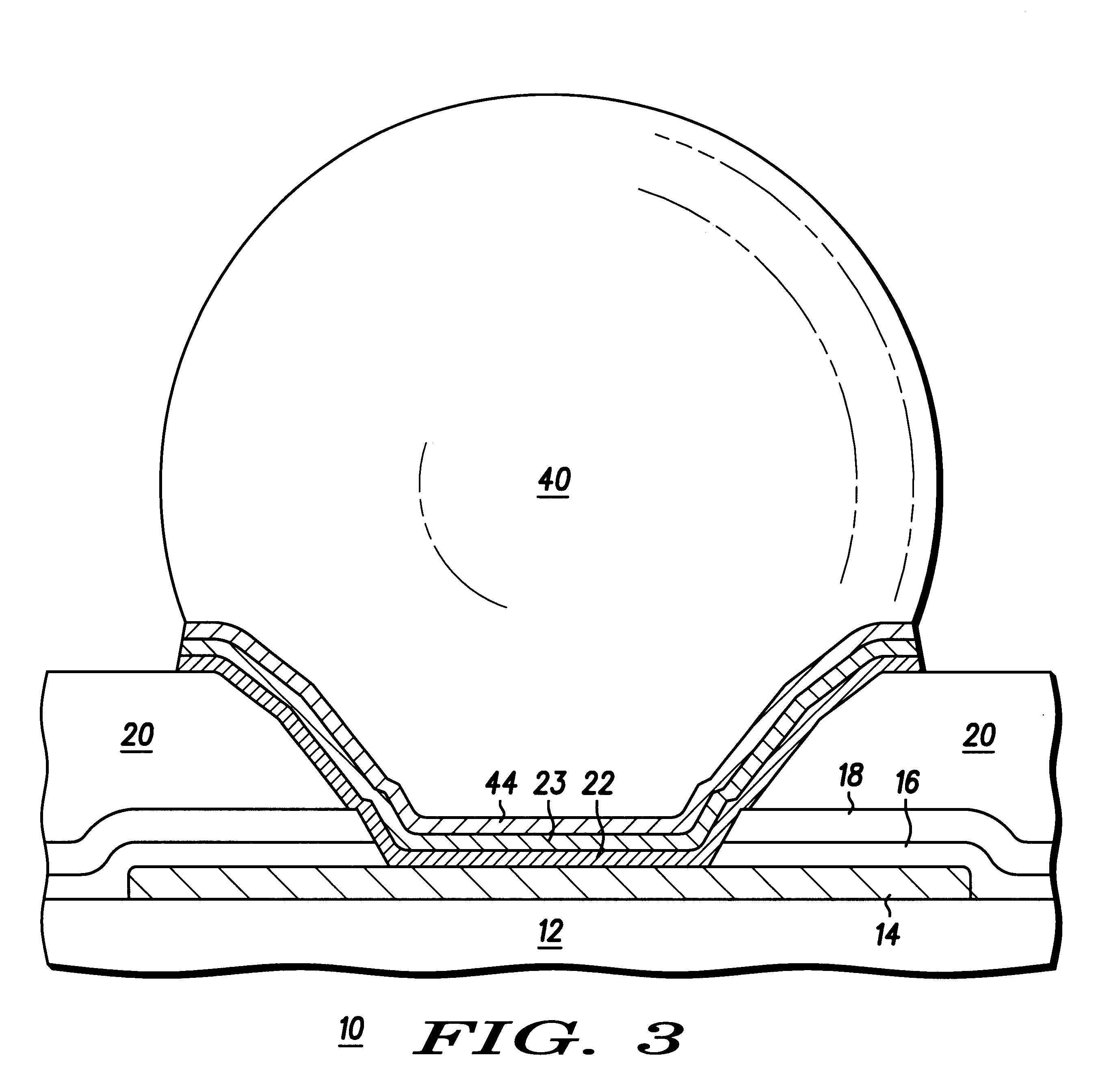
The present invention provides a method for eliminating the gold layer that is traditionally formed on top of a copper layer in a UBM stack. Gold has been used for over 30 years in evaporative solder bump processes for the purpose of preventing oxidation of the underlying copper layer. Copper, upon exposure to ambient air, forms a native oxide layer which impairs adhesion of the bump to the UBM and, because it is a dielectric, also results in poor electrical characteristics of the bumps. The present invention provides a method in which gold can be eliminated and problems associated with copper oxidation can be overcome. Although the discussion herein specifies solder bumps, other conductive materials besides solder may be utilized. In one form, after the copper layer of the UBM is deposited, the semiconductor substrate is exposed to ambient air as a consequence of moving from one processing tool to another in which a vacuum environment cannot be maintained. As a result, a copper oxi...


PUM

PropertyMeasurementUnit
temperatureaaaaaaaaaa
thicknessaaaaaaaaaa
thicknessaaaaaaaaaa

Abstract

A semiconductor device (10) includes a solder bump (40) that is formed using a gold-free under-bump metallurgy (UBM) (21). In a preferred embodiment, UBM (21) includes a diffusion barrier layer (22) of chromium and a metallic layer (24) of copper. The bump layer metallurgy (31) is deposited directly on the metallic layer, without an intervening gold layer. To overcome problems associated with a native oxide layer (26) which forms on the metallic layer, especially on copper, the bump metallurgy includes a seed layer (32) of tin that is deposited prior to a bulk lead layer (34). The bump metallurgy includes a final metallic layer (36) having sufficient tin to make a bump having approximately 97% Pb and 3% tin.

Description

This invention relates in general to semiconductor devices and their method of formation, and more particularly to semiconductor devices having solder bumps and methods for forming the solder bumps.Background of the Invention Controlled Collapse Chip Connection (C4) interconnect technology is one form of flip-chip bump technology which is an alternative to wire bonding. The C4 interconnect process involves forming solder bumps and under-bump metallurgy (UBM) structures on a semiconductor chip's bond pads. The solder bumps are used in place of wires to electrically connect the chip's circuitry to external sources, for example to substrates used for chip packaging. The UBM provides important functions with respect to the C4 structure, among them include providing adhesion, electric continuity, and barrier protection between the C4 solder bump and semiconductor chip.Conventional high-lead C4 solder bumps (solder bumps containing 97% lead and 3% tin) use a UBM integration that consists ...

Claims


Application Information

Patent Timeline
Patent Type & Authority Patents(United States)
IPC IPC(8): H01L21/02H01L21/60
CPCH01L24/03H01L24/05H01L24/11H01L2224/0401H01L2224/05599H01L2224/13099H01L2224/131H01L2924/01005H01L2924/01006H01L2924/01013H01L2924/01014H01L2924/01022H01L2924/01027H01L2924/01028H01L2924/01029H01L2924/0105H01L2924/01074H01L2924/01078H01L2924/01079H01L2924/01082H01L2924/01327H01L2924/014H01L2924/05042H01L2924/01024H01L2924/01033H01L2924/00014H01L2224/11502H01L2224/11849
Inventor SHERIDAN, DEVIN ROBERTLARSEN, LARRY J.KNAUSS, MARTIE D.
Owner NXP USA INC
Why Eureka
Try Eureka