

Spiral inductor semiconducting device with grounding strips and conducting vias
a semiconducting device and spiral inductor technology, applied in the direction of inductance, transformer/inductance coil/winding/connection, inductance, etc., can solve the problem of excessive power loss, undesirable power loss, and reduce the selectivity of resonant circuits. problem, to achieve the effect of preserving the useful operation of the inductor over a wider rang
- Summary
- Abstract
- Description
- Claims
- Application Information
AI Technical Summary
Benefits of technology
Problems solved by technology
Method used
Image

Examples
Embodiment Construction
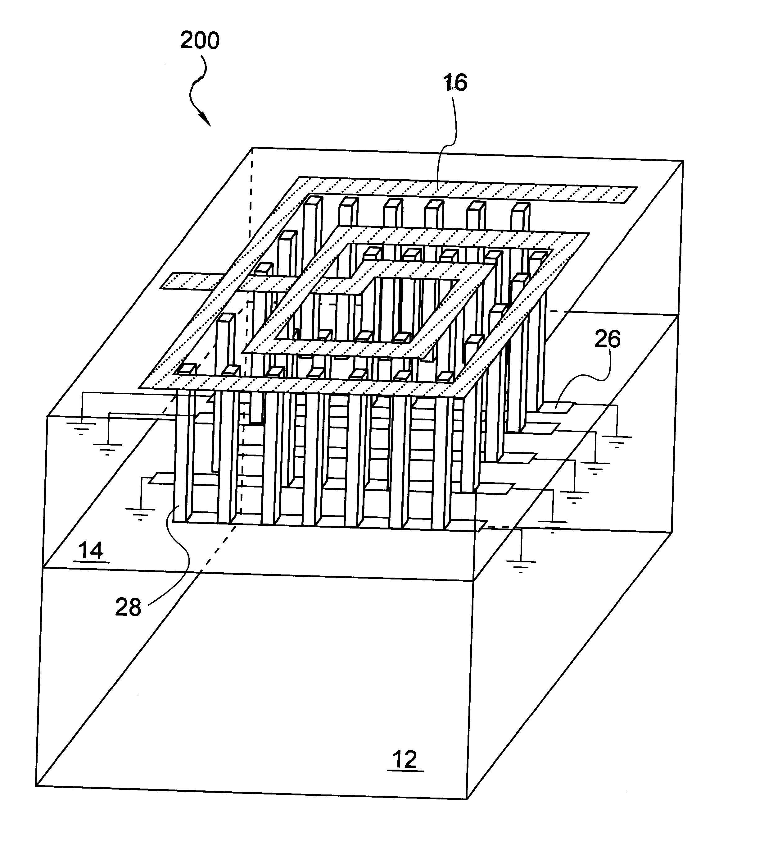
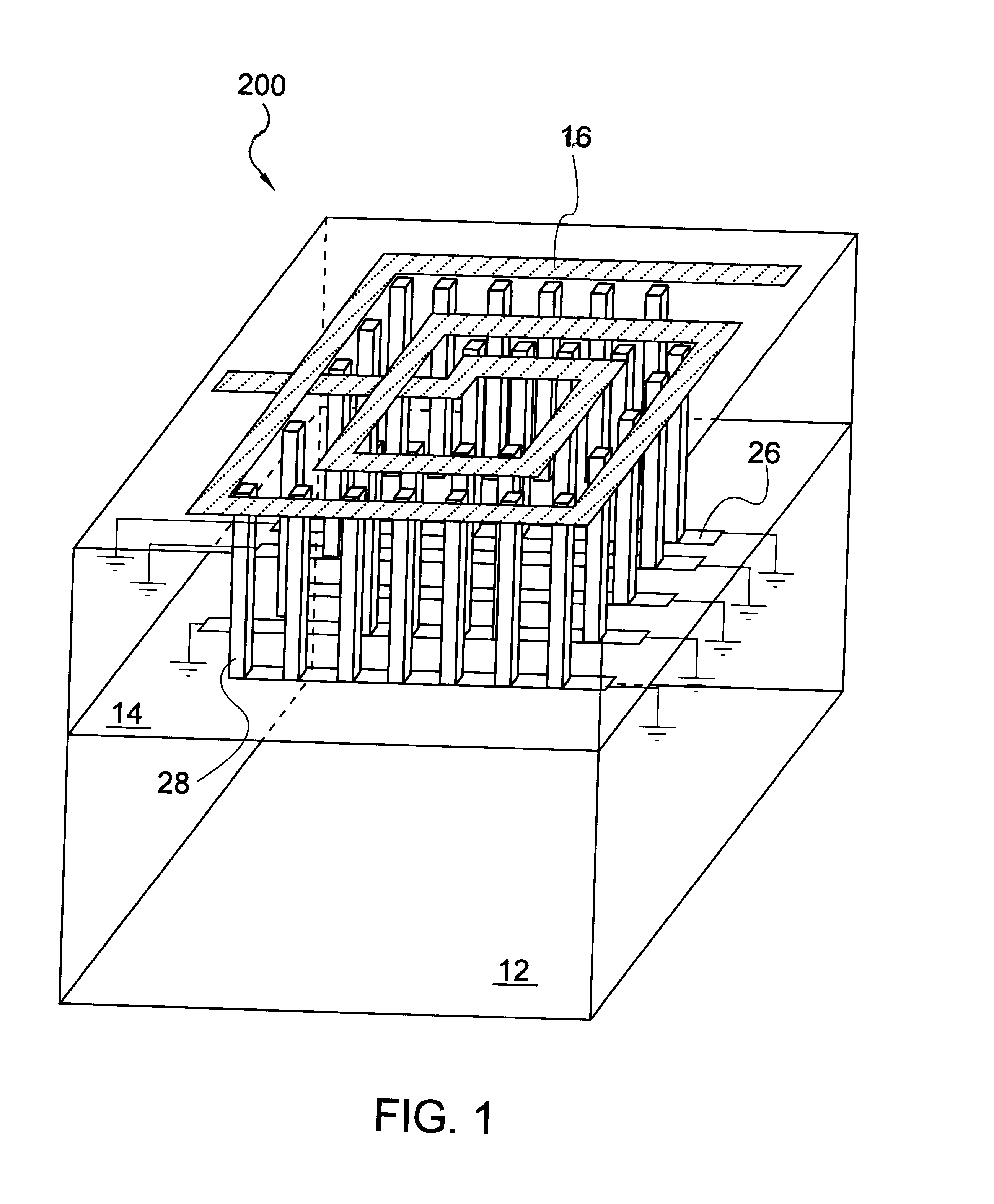
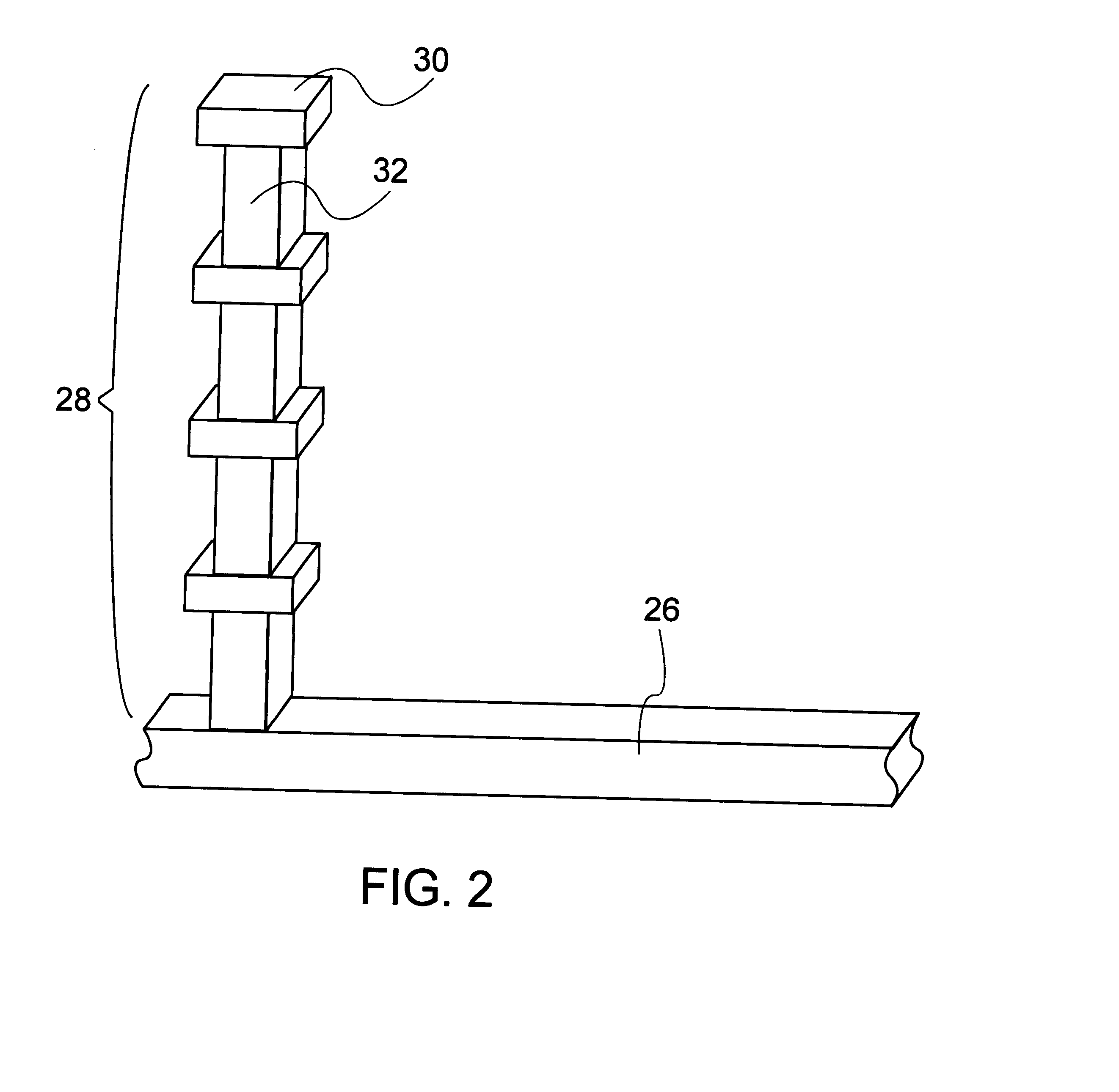
According to the present invention, a semiconducting device is provided comprising a ground plane disposed between a spiral inductor and a conductive substrate. The ground plane is cut into a plurality of ground strips in order to prevent the flow of image current that would be induced in a solid ground plane by the magnetic field of the inductor. The ground strips are capacitively linked to the inductor by multiple conducting vias. These conducting vias are preferably formed out of a low-resistivity metal like copper or aluminum and act to terminate the parasitic electric field without excessively increasing the capacitance to ground. In a preferred embodiment, fabrication of the conducting vias into the back-end-of-line (BEOL) metallurgy is accomplished by simply adding the chain via patterns to existing mask level designs and performing standard damascene fill processes as is currently practiced to form test via chains.
Referring now to FIG. 1, which shows the present invention, i...
PUM
 Abstract
Description
Claims
Application Information