Plasma apparatus and lower electrode thereof

a technology which is applied in the field of plasma apparatus and lower electrode thereof, can solve the problems of contaminating the wafer surface, dust generation, and inability to use vacuum adsorption to hold a substrate, so as to achieve the effect of preventing abnormal discharge and most efficiently preventing abnormal discharg

Inactive Publication Date: 2002-12-10
TOKYO ELECTRON LTD
View PDF5 Cites 54 Cited by
  • Summary
  • Abstract
  • Description
  • Claims
  • Application Information

AI Technical Summary

Benefits of technology

Since the capacitor is interposed, it is possible to control the phases of the high frequency powers to be applied to the electrode of the electrostatic adsorption member and the base table. If the phase difference is reduced to a minimum, the abnormal disch...

Problems solved by technology

However, when processing is performed under the high vacuum, vacuum adsorption cannot be used for holding a substrate such as a semiconductor substrate (hereinafter referred to as "wafer") since the vacuum adsorption is usually applicable in the air.
As a result, dust is...

Method used


Image

  • Plasma apparatus and lower electrode thereof
  • Plasma apparatus and lower electrode thereof
  • Plasma apparatus and lower electrode thereof

Examples


Embodiment Construction

Now, embodiments of the present invention will be described more specifically.

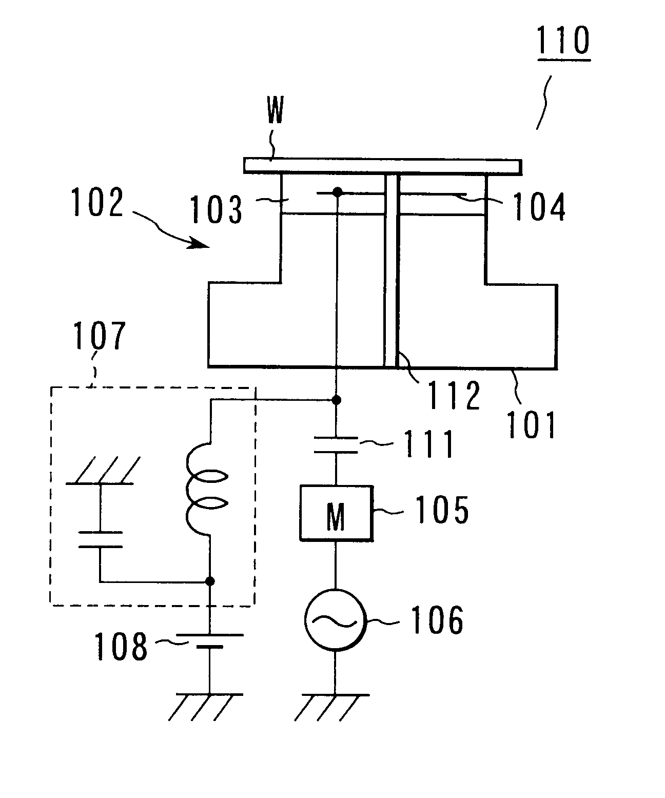
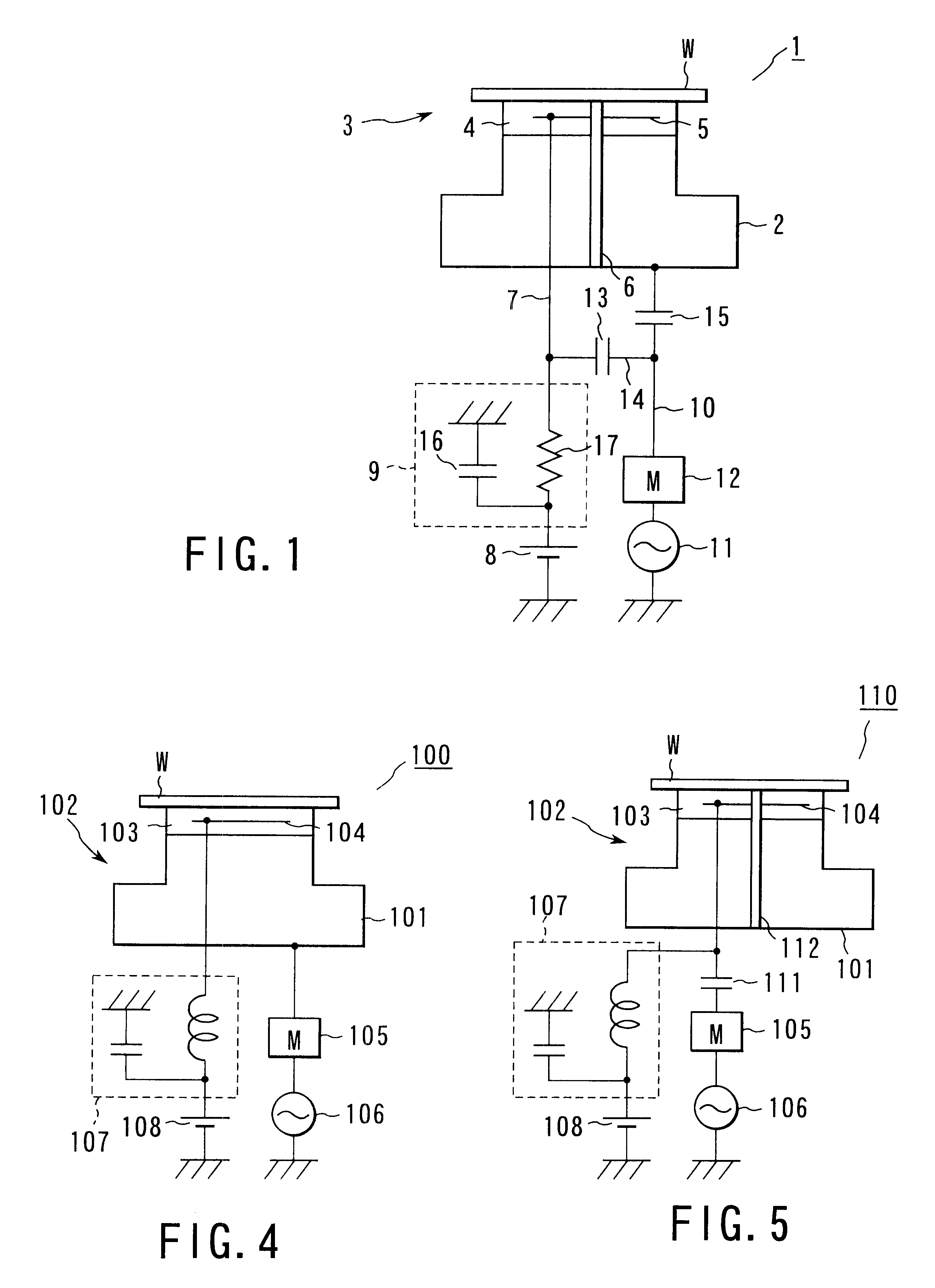
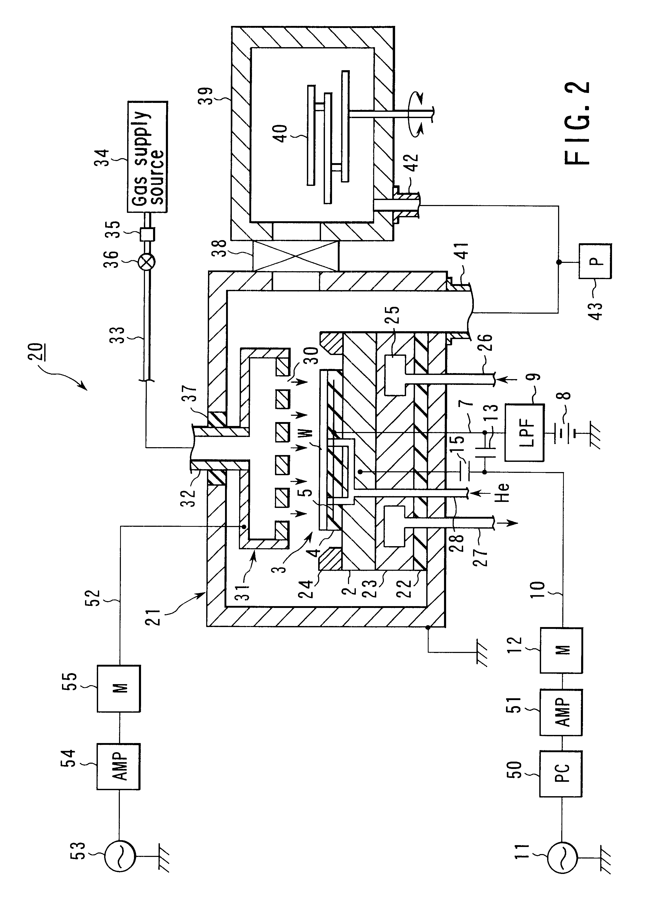
FIG. 1 is a schematic view of a lower electrode structure according to an embodiment of the present invention.

A lower electrode structure 1 shown in FIG. 1 is arranged in an chamber of a plasma processing apparatus such as a plasma etching apparatus and serves as a plasma formation electrode.

The lower electrode structure 1 has a base table formed of a conductive material such as aluminium, namely, a susceptor 2. On the susceptor 2, formed is an electrostatic chuck 3 (electrostatic adsorption member) having a dielectric layer 4 and a flat electrode 5 arranged inside the dielectric layer.

As materials for forming the dielectric layer 4, there are ceramic and a resin. The dielectric layer 4 formed of ceramic is particularly effective in this embodiment.

A pipe 6 for supplying a heat-transmitting gas such as helium (He) is vertically formed through the susceptor 2 and the dielectric layer 4. The pipe 6 is branch...


PUM

PropertyMeasurementUnit
Dielectric polarization enthalpyaaaaaaaaaa
Electrical conductivityaaaaaaaaaa
Currentaaaaaaaaaa

Abstract

The present invention is constituted of a lower electrode structure (1) comprising a base table (2) formed of a conductive material, an electrostatic adsorption member (3) formed on the base table (2) and having a dielectric layer (4) on which the substrate to be mounted and within which an electrode (5) electrically isolated from the base table (2) is housed, first wiring (7) having an end connected to the electrode (3) of the electrostatic adsorption member, a direct-current source (8) connected to the other end of the first wiring (7), second wiring (10) having an end connected to the base table (2), a high frequency source (11) connected to the other end of the second wiring (10), a third wiring (14) for connecting the first wiring (7) and the second wiring (10), and a capacitor (13) formed on the third wiring (14). Plasma processing is performed by disposing the lower electrode structure (1) in the chamber (21).

Description

The present invention relates to a lower electrode structure used in applying plasma processing, such as etching, to a substrate such as a semiconductor substrate. The present invention also relates to a plasma processing apparatus using the lower electrode structure.In a manufacturing process for a semiconductor device etc., processing within a high vacuum, such as a plasma etching, is frequently employed. However, when processing is performed under the high vacuum, vacuum adsorption cannot be used for holding a substrate such as a semiconductor substrate (hereinafter referred to as "wafer") since the vacuum adsorption is usually applicable in the air. For this reason, the wafer is usually held by a mechanical means such as a clamp.When the wafer is held by the clamp, the distal end of the clamp comes into contact with an edge or a working surface of the wafer. As a result, dust is generated at the time the clamp comes into contact with the wafer and sometimes contaminates the wafe...

Claims


Application Information

Patent Timeline
IPC IPC(8): B23K10/00H01L21/68H01L21/02H01L21/67H01L21/3065
CPCH01L21/67069H01L21/6833H01L21/3065
Inventor TAGUCHI, CHIHIRONONAKA, RYO
Owner TOKYO ELECTRON LTD
Why Eureka
Try Eureka