

Piezoelectric element and manufacturing method and manufacturing device thereof
a piezoelectric element and manufacturing method technology, applied in the field of piezoelectric elements, can solve the problems of difficult to obtain the orientation degree of a piezoelectric element in a stable manner, achieve stable and superior piezoelectric properties, and facilitate reproducibility
- Summary
- Abstract
- Description
- Claims
- Application Information
AI Technical Summary
Benefits of technology
Problems solved by technology
Method used
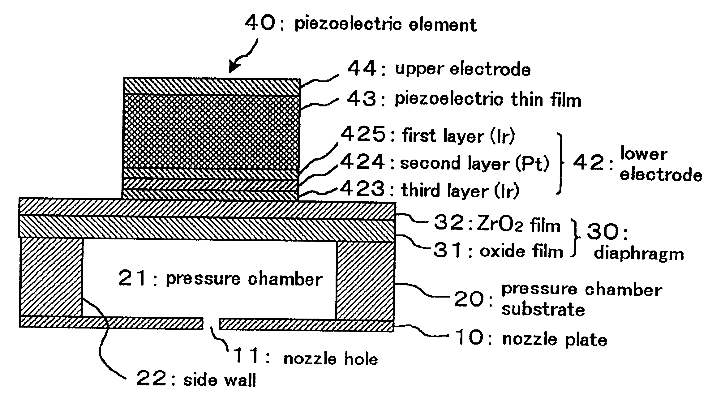
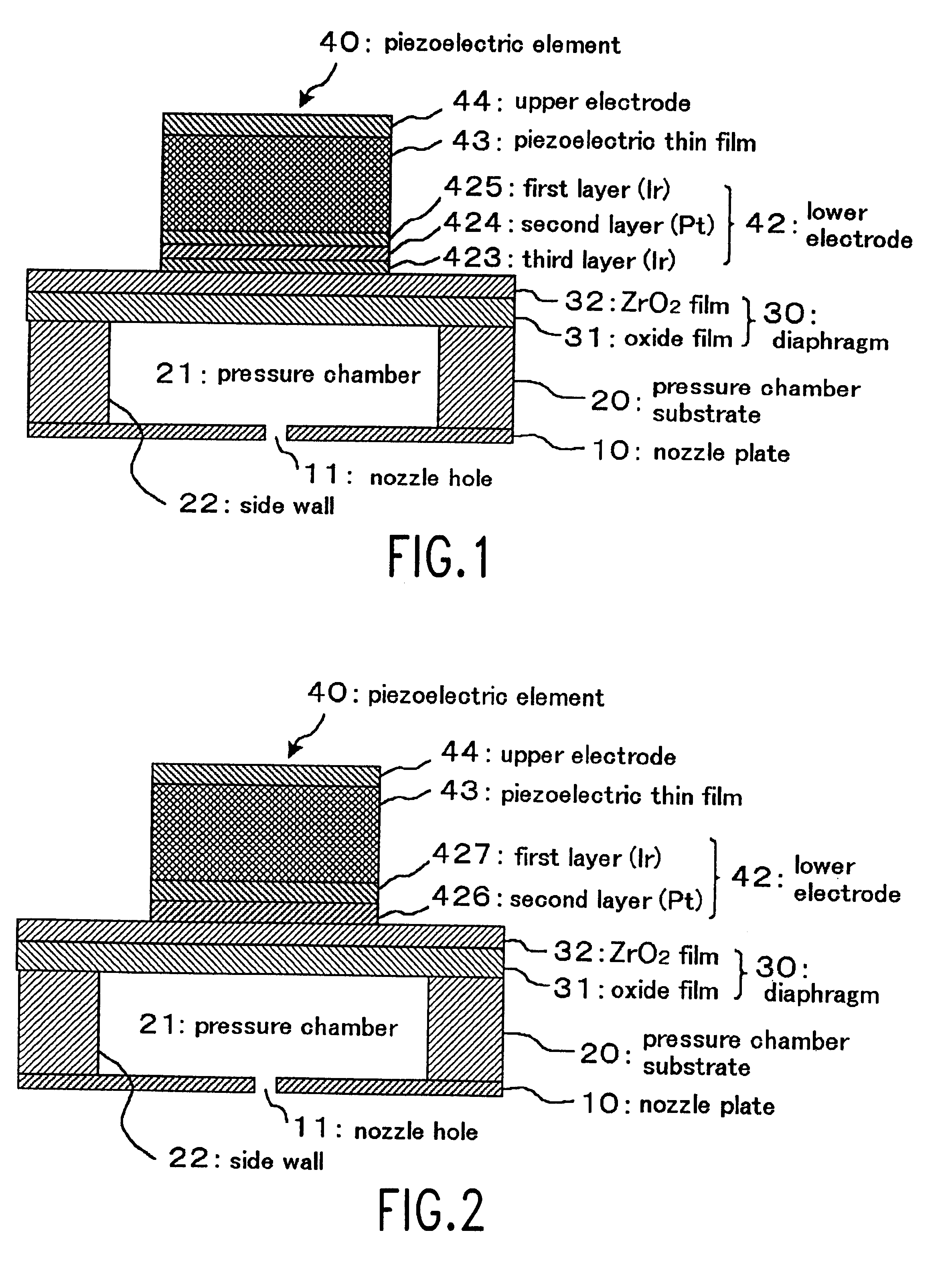
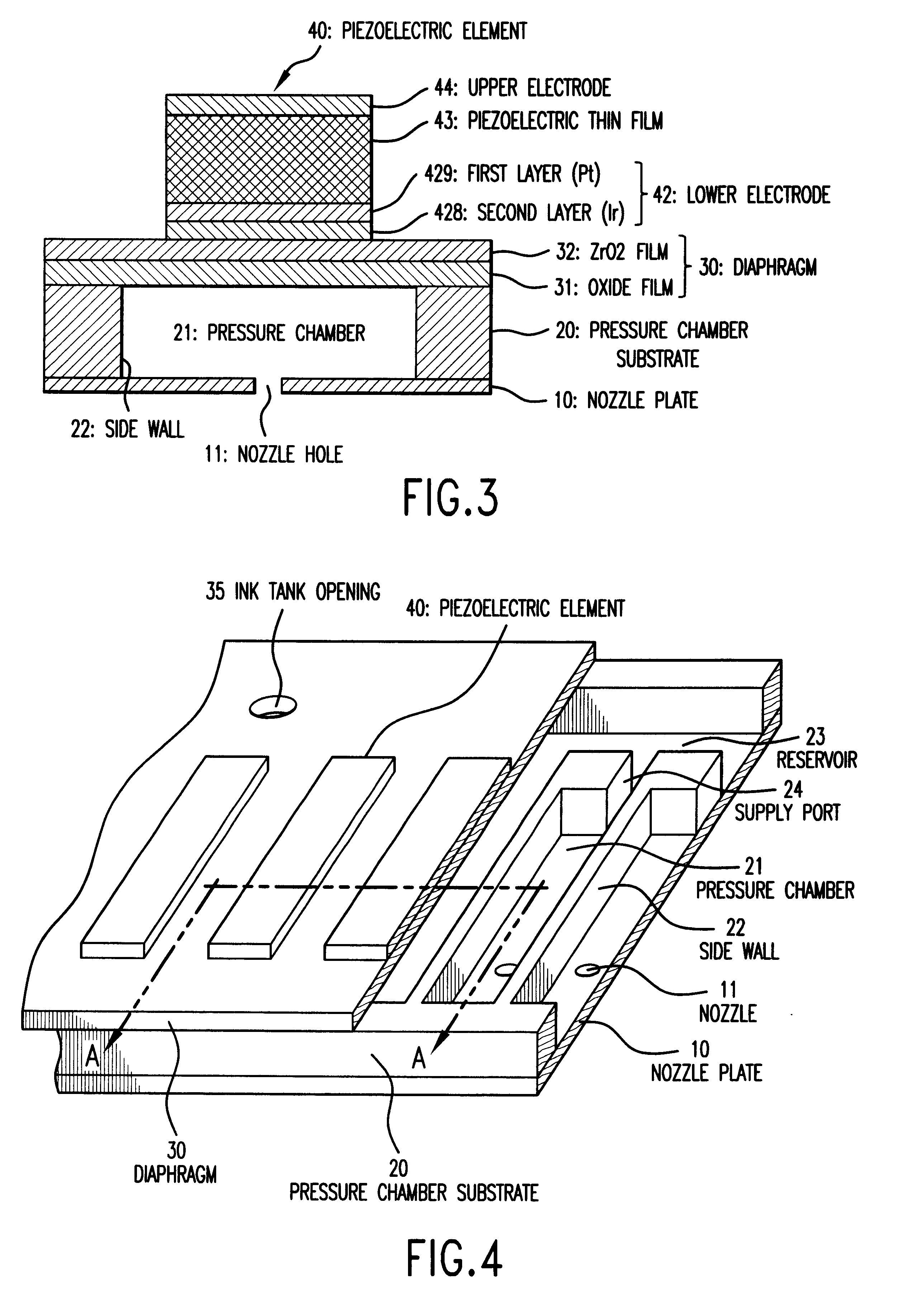
Image

Examples
example 4-2
Another piezoelectric element was manufactured in accordance with the manufacturing method of the present embodiment. In particular, the thickness of the aforementioned titanium layer formed on the lower electrode 42 was set to 15 nm in order to control the piezoelectric thin film to be of a desired crystal orientation. In other words, the layer structure below the piezoelectric precursor layer 43' was made to be Ti 15 nm / Ir 20 nm / Pt 140 nm / Ir 20 nm / Ti 10 nm / ZrO.sub.2 400 nm. Upon crystallizing this substrate with heat treatment, the piezoelectric thin film is preferentially oriented toward the (111) face under the influence of the aforementioned layer structure. As a practical matter, the (100) face half value breadth of the piezoelectric thin film, which was obtained by applying heat from the lower electrode side, was measured with the X-ray diffraction angle method, and the piezoelectric constant of such piezoelectric thin film when constituting an inkjet head was also measured. ...
modification examples
Other Modification Examples
The present invention may be modified and adapted in various forms without restriction to the aforementioned embodiments. For instance, in addition to being adaptable as the piezoelectric element of the aforementioned inkjet recording head, the piezoelectric element manufactured according to the present invention can also be employed in the manufacture of non-volatile semiconductor memory devices, thin film condensers, pyroelectricity detectors, sensors, surface acoustic wave optical wave guides, optical memory devices, space optical modulators, ferroelectric devices such as a frequency duplicator for diode lasers, dielectric devices, pyroelectric devices, piezoelectric devices, and electro-optic devices.
PUM
 Abstract
Description
Claims
Application Information