Method of fabricating memory cell structure of flash memory having annular floating gate

a technology of floating gate and memory cell, which is applied in the field of flash memory, can solve the problems of deteriorating the quality and reliability of flash memory, affecting the operation of flash memory, and difficulty in controlling the number of electrons released from the floating ga

Inactive Publication Date: 2003-02-11
WEN WEN YING
View PDF13 Cites 20 Cited by
  • Summary
  • Abstract
  • Description
  • Claims
  • Application Information

AI Technical Summary

Benefits of technology

The primary object of the present invention is to provide a flash memory structure and a method for fabricating the same. In the proposed flash memory, an annular floating gate situated between the drain and the source is exploited. An interpoly dielectric and a control gate are stacked on the surface of the floating gate and on the gate oxide exposed at the center of the floating gate by means of self-alignment. Thereby above mentioned problem can be overcome, and reliability of devices can be enhanced.
Another object of the present invention is to provide a flash memory structure and a method for fabricating the same. In the proposed flash memory, an interpoly dielectric and a control gate circumvent the periphery of the floating gate to enhance the capacitance coupling ratio between the control gate, the floating gate, and the source. Memory cells of the flash memory having efficient program process of writing or erase process can thus be obtained.
Yet another object of the present invention is to provide a flash memory structure and a method for fabricating the same. In the proposed flash memory, the interpoly dielectric circumventing the floating gate is an oxide / nitride / oxide (ONO) structure or an oxide / nitride (ON) structure. The quality and thickness of the interpoly dielectric can be exactly controlled. Flash memory cells of high capacitance coupling ratio and low leakage current can thus be produced.
Yet another object of the present invention is to provide a flash memory structure and a method for fabricating the same. In the proposed flash memory, the floating gate and the source and the drain are electrically insulated by a thicker oxide to reduce accuracy requirement of the fabrication process and to enhance reliability of devices.
Yet another object of the present invention is to provide a flash memory structure and a method for fabricating the same. The proposed fabrication method is compatible to the general fabrication process of CMOS devices, thus simplifying the fabrication process.

Problems solved by technology

However, for a flash memory of stacked gate type, it is difficult to control the number of electrons released from the floating gate 15 during the data-erasing procedure.
Over erase may easily arise, deteriorating the quality and reliability of the flash memory.
Therefore, the area of memory cell thereof will be large so that integration density of memory cell can not be effectively increased.
Additionally, although a thinner tunneling oxide can enhance the tunneling effect of electrons, it is very difficult to fabricate a thin oxide having high tunneling effect of electrons in low-power non-volatile memory devices.
Moreover, leakage current resulted from increased defect density and stress defects may easily arise to deteriorate the reliability of devices.

Method used


Image

  • Method of fabricating memory cell structure of flash memory having annular floating gate
  • Method of fabricating memory cell structure of flash memory having annular floating gate
  • Method of fabricating memory cell structure of flash memory having annular floating gate

Examples


Embodiment Construction

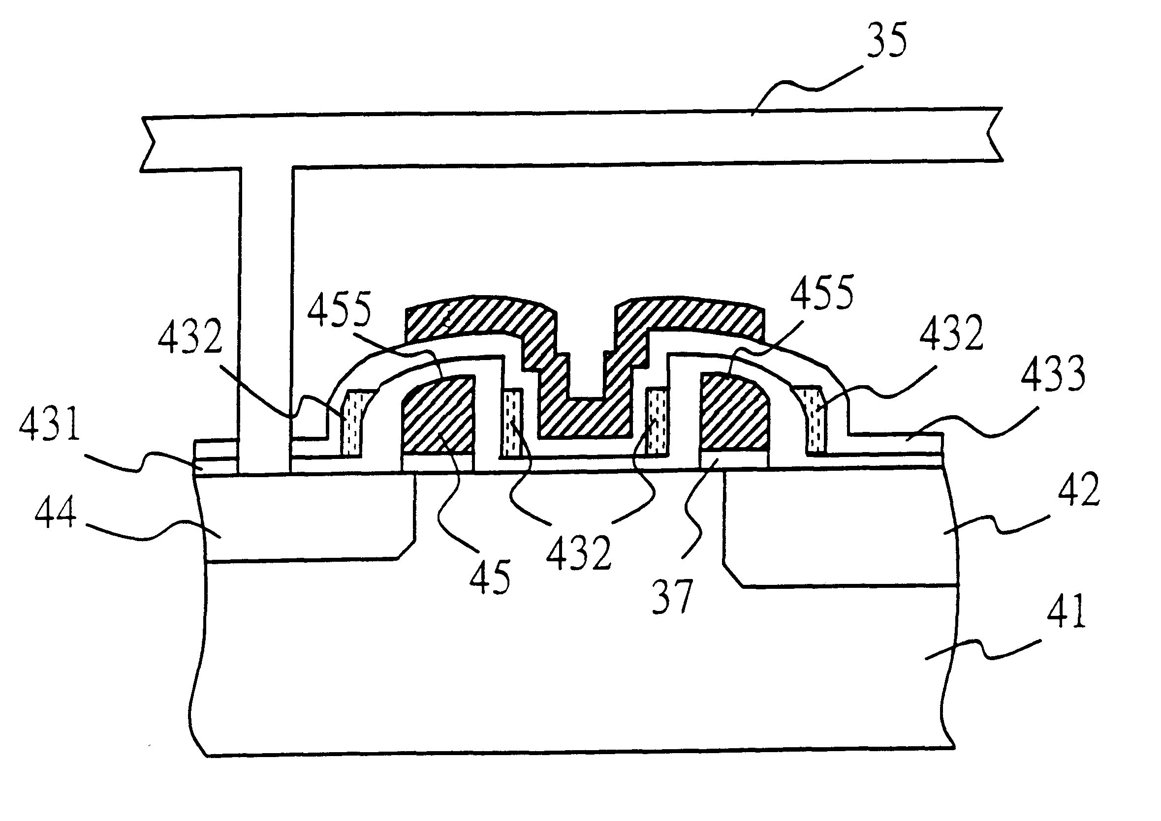
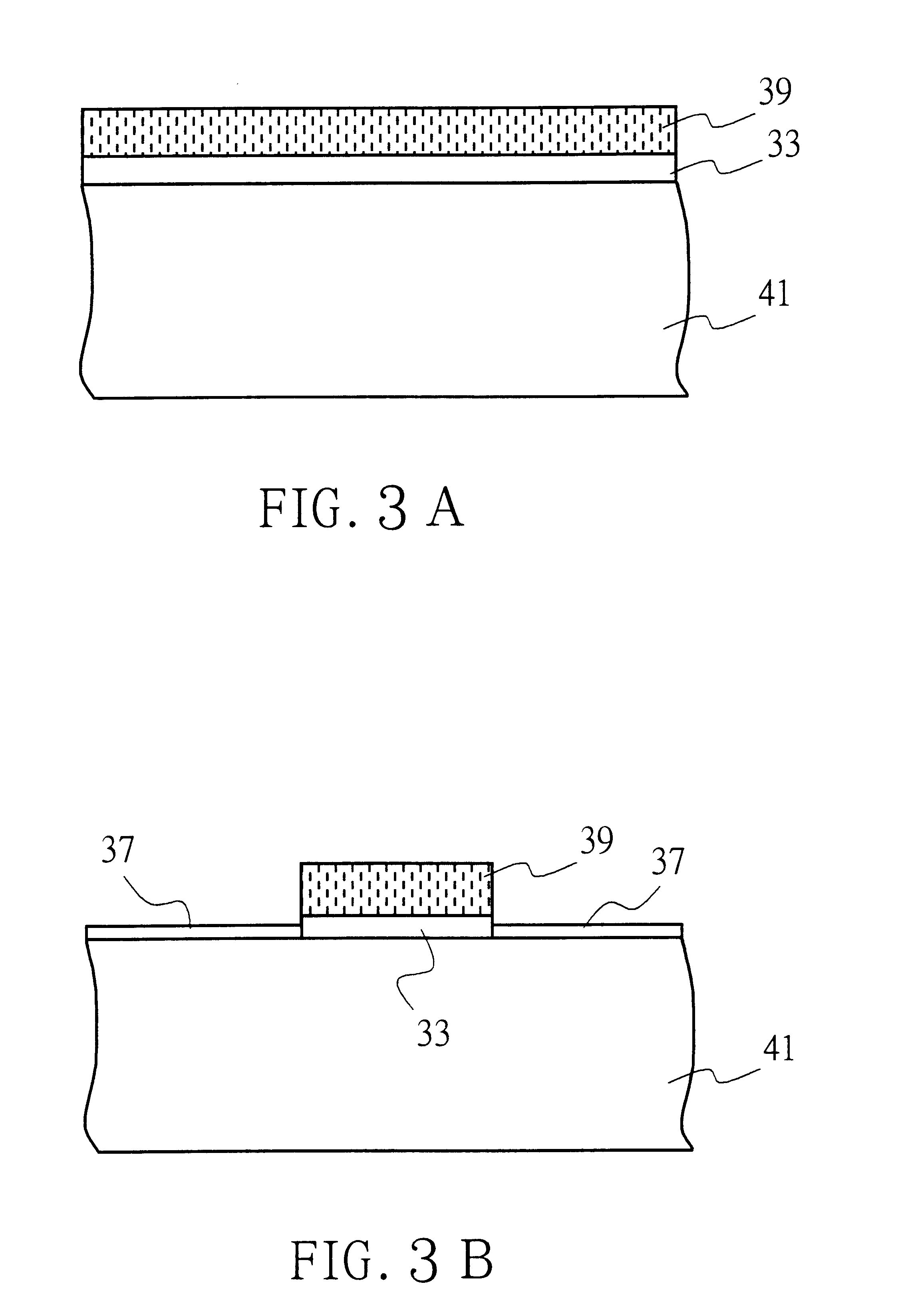
As shown in FIGS. 3A to 3H, the fabrication method of a memory cell according to a preferred embodiment of the present invention comprising the steps of:

Step A (as shown in FIG. 3A): providing a semiconductor substrate 41; forming a pad oxide 33 and a SiN 39 on the surface of the substrate 41; forming a plurality of field oxides (FOX) 31 in specific regions of the substrate 41 by the techniques of photolithography, etching, and oxidation (The action area of the memory cell can be defined between two field oxides 31.),

Step B (as shown in FIGS. 3B and 4A): etching out the patterns of the pad oxide 33 and the SiN 39 to reserve only parts thereof situated between two field oxides 31 by the photolithography and etching techniques; forming a gate oxide 37 with a thickness larger than that of the tunneling oxide in prior art on the surface of the substrate 41 not covered by the SiN 39,

Step C (as shown in FIG. 3C): forming a poly-silicon 45 on the surface of each region,

Step D (as shown in ...


PUM


Abstract

The present invention relates to a memory cell structure of a flash memory and a method for fabricating the same and, more particularly, to a flash memory having annular floating gates. The present invention uses the capacitance coupling between the source and the floating gate to form a channel in the substrate under the floating gate. Hot electrons are injected into the floating gate or released from the floating gate to the control gate through inerpoly dieletric by injection point on the top of floating gate In the proposed memory cell, a floating gate is etched to form an annular shape situated between a drain, a source, and two field oxides. An interpoly dielectric and a control gate are stacked in turn on the floating gate and on the surface of the substrate not covered by the floating gate through means of self-alignment. An injection point not covered by the SiN film of the interpoly dielectric is formed on the top of the floating gate. Thereby the present invention can not only achieve self-alignment to form the control gate and apply to high-integration memory cells with small areas, but also can release electrons from the floating gate to the control gate by the FN tunneling effect to effectively increase efficiency of erasing data and reliability of devices.

Description

The present invention relates to a memory cell structure of a flash memory and a method for fabricating the same and, more particularly, to a flash memory having annular floating gates. The present invention uses the capacitance coupling between the source and the floating gate to form a channel in the substrate under the floating gate. Hot electrons are injected into the floating gate or released from the floating gate to the control gate through inerpoly dieletric by injection point on the top of floating gate.Flash memories have been widely used in electronic products such as portable computers or communication apparatuses because of their non-volatile functions of electrically writing and erasing. Flash memories can generally be categorized into two types according to the shape of their gates: the stacked gate type and the split gate type.FIG. 1 shows a cross-sectional view of a memory cell of a flash memory of stacked gate type in prior art. As shown in the figure, a stacked ga...

Claims


Application Information

Patent Timeline
Patent Type & Authority Patents(United States)
IPC IPC(8): H01L21/28H01L29/66H01L21/336H01L29/40H01L21/02H01L29/423H01L29/788G11C16/04
CPCH01L21/28273H01L29/7885H01L29/66825H01L29/42324G11C16/0425H01L29/40114
Inventor WEN, WEN YING
Owner WEN WEN YING
Why Eureka
Try Eureka