Doping of thin amorphous silicon work function control layers of MOS gate electrodes

a technology of mos gate electrodes and mos, which is applied in the direction of basic electric elements, electrical apparatus, and semiconductor devices, can solve the problems of reducing performance by about 15% or more, adversely affecting polysilicon gates, and increasing the effective gate oxide thickness ("eot")

Inactive Publication Date: 2003-02-11
ADVANCED MICRO DEVICES INC
View PDF13 Cites 72 Cited by
  • Summary
  • Abstract
  • Description
  • Claims
  • Application Information

AI Technical Summary

Problems solved by technology

However, polysilicon-based gate electrodes incur a number of disadvantages, including, inter alia: (1) as device design rules decrease to below about 0.20 .mu.m, polysilicon gates are adversely affected by poly depletion, wherein the effective gate oxide thickness ("EOT") is increased.
Such increase in EOT can reduce performance by about 15% or more; (2) polysilicon-based gate electrodes have higher resistivities than most metal or metallic materials and thus devices including polysilicon as electrode or circuit materials operate at a much slower speed than equivalent devices utilizing metal based materials.
Further, a significant portion of the voltage applied to the gate during operation is dropped in the polysilicon due to the poor conductivity of silicon.
The use of metal or metallic materials as replacements for polysilicon-based materials as gate electrodes in MOS and/or CMOS devices incurs several difficulties, however, which difficulties must be considered and overcome in any metal-based gate electrode process scheme, including: (1) metal and/or metal-based gates cannot withstand the higher temperatures and oxidative ambients which conventional polysilicon-based gate electrode materials can withstand; (2) several candidate metals or metallic materials for use as gate electrodes do not exhibit adequate adhesion in film form to surrounding layers of different materials when these metals or metallic materials are patterned to very small geometries; (3) some metal or metallic films are difficult to lithographically pattern and etch via conventio

Method used


Image

  • Doping of thin amorphous silicon work function control layers of MOS gate electrodes
  • Doping of thin amorphous silicon work function control layers of MOS gate electrodes
  • Doping of thin amorphous silicon work function control layers of MOS gate electrodes

Examples


Embodiment Construction

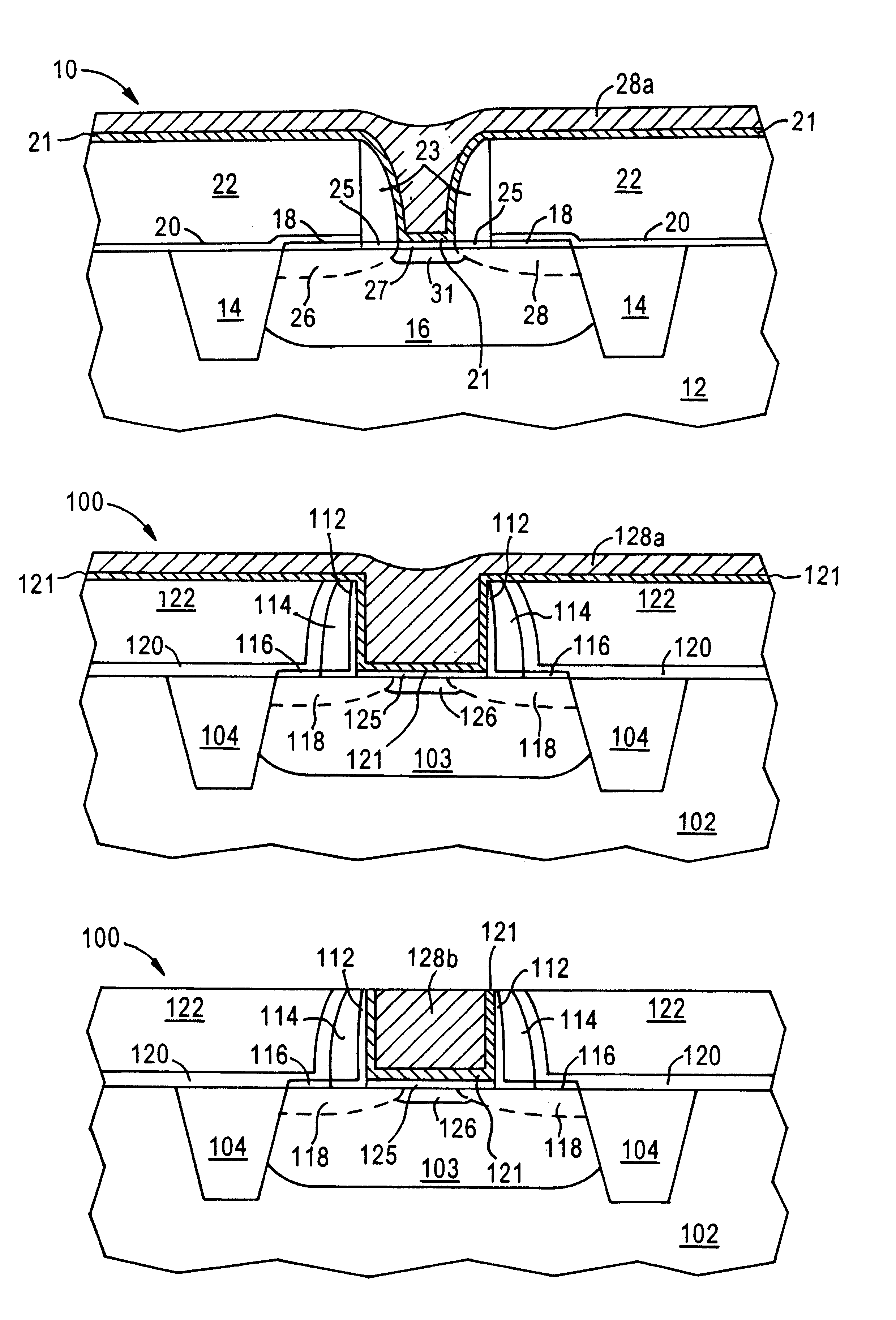
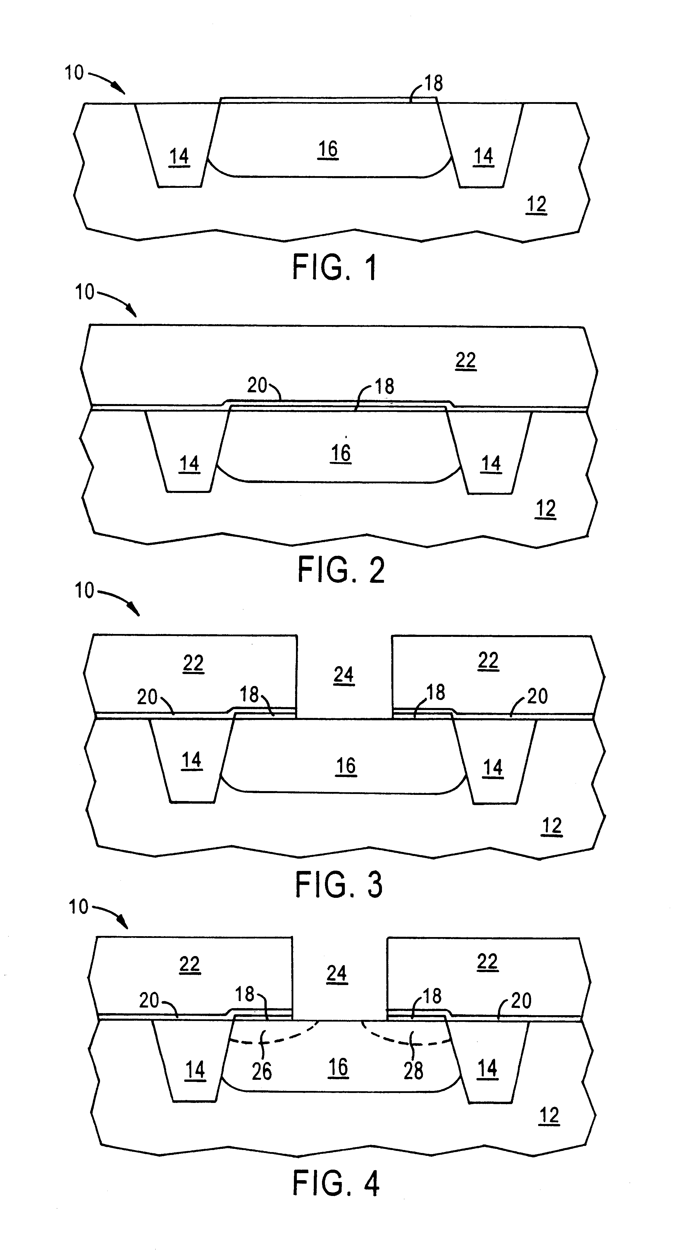
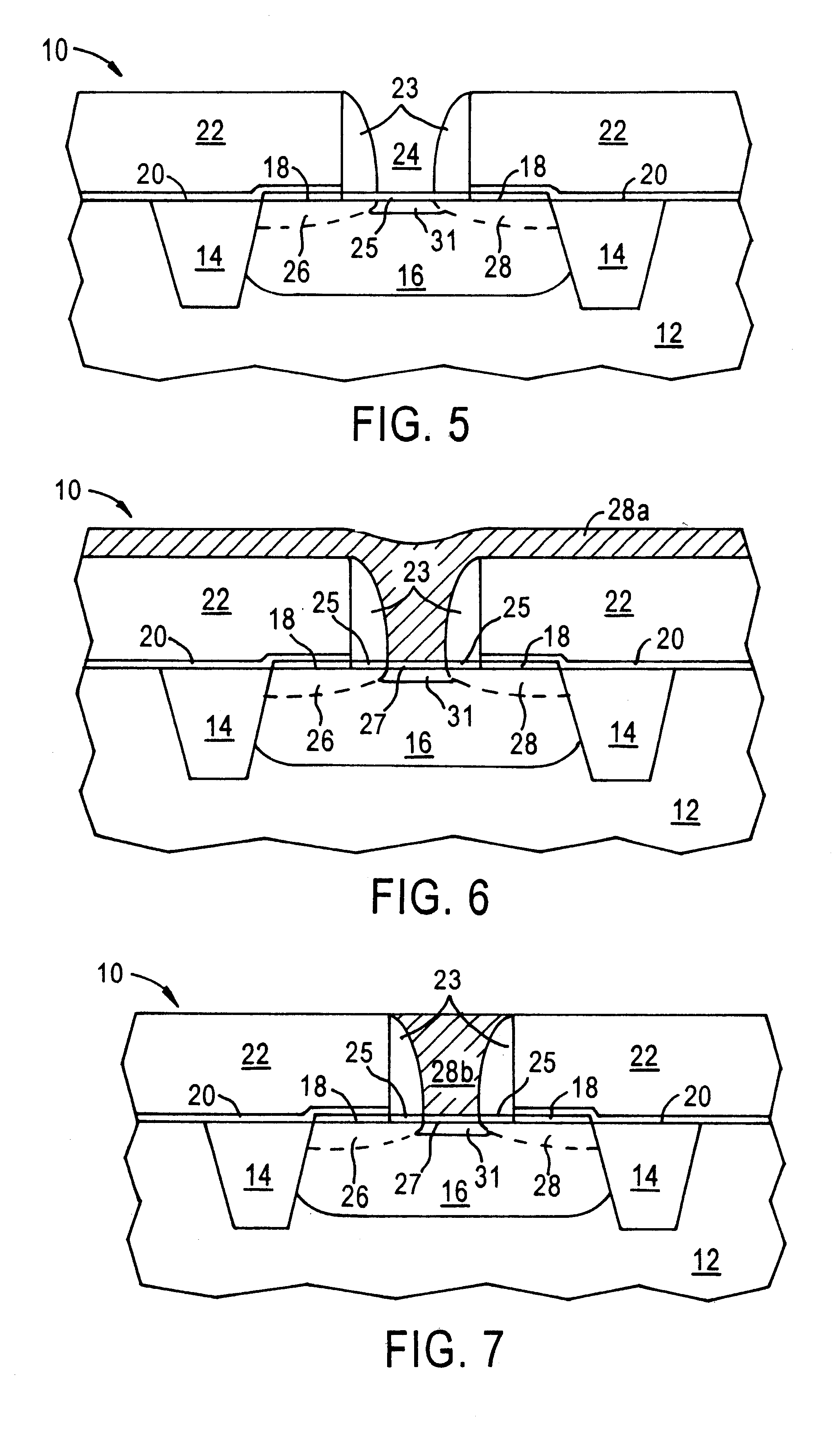
The present invention is based upon the discovery that thin, doped Si layers for use as work function control / adjust layers intermediate an in-laid metal electrode and an underlying thin gate insulator layer of a MOS transistor and / or CMOS device, can be readily formed by a process which prevents, or at least substantially reduces, damage to the thin gate insulator layer and doping of the underlying channel region within the semiconductor substrate characteristic of the conventional dopant implantation-based methodology. A key feature of the present invention is the initial formation of a thin amorphous Si ("a-Si") layer over the thin gate insulator layer, rather than a polycrystalline Si layer as in conventional practice. The thin amorphous Si layer, in contrast with the conventional polycrystalline Si layer, facilitates doping by means of a low energy process, e.g., plasma doping at a low sheath voltage, and thus advantageously avoids, or at least minimizes, the damage to the thin...


PUM


Abstract

Work function control layers are provided in in-laid, metal gate electrode, Si-based MOS transistors and CMOS devices by a process which avoids deleterious dopant implantation processing resulting in damage to the thin gate insulator layer and undesirable doping of the underlying channel region. According to the invention, an amorphous Si layer is formed over the thin gate insulator layer by a low energy deposition process which does not adversely affect the gate insulator layer and subsequently doped by means of another low energy process, e.g., low sheath voltage plasma doping, which does not damage the gate insulator layer or dope the underlying channel region of the Si-based substrate. Subsequent thermal processing during device manufacture results in activation of the dopant species and conversion of the a-Si layer to a doped polycrystalline Si layer of substantially increased electrical conductivity.

Description

The present invention relates to methods of manufacturing semiconductor devices including a gate electrode, e.g., MOS transistors and CMOS devices. More specifically, the present invention relates to methods of manufacturing MOS and CMOS semiconductor devices wherein the source, drain, channel regions, and the gate electrodes of MOS transistors are formed in a self-aligned manner utilizing an in-laid ("damascene") gate and corresponding processing techniques therefor. The present invention has particular utility in the manufacture of high integration density semiconductor devices employing design rules of 0.20 .mu.m and below, e.g., 0.15 .mu.m and below.BACKGROUND OF THE INVENTION AND RELATED ARTThe escalating requirements for high density and performance (e.g., transistor and circuit speeds) associated with ultra-large scale integration ("ULSI") devices necessitate design rules for component features of 0.20 .mu.m and below, such as 0.15 .mu.m and below, such as source, drain, and ...

Claims


Application Information

Patent Timeline
IPC IPC(8): H01L21/70H01L21/8238
CPCH01L21/823842Y10S438/923
Inventor BUYNOSKI, MATTHEW S.
Owner ADVANCED MICRO DEVICES INC
Why Eureka
Try Eureka