
Microwave field effect transistor structure on silicon carbide substrate

a microwave field and transistor technology, applied in the direction of semiconductor devices, semiconductor/solid-state device details, electrical devices, etc., can solve the problems of limiting the thermal dissipation of silicon-built devices, affecting the growth and device fabrication technology, and limiting the experience of silicon-built devices. the effect of thermal dissipation

Inactive Publication Date: 2003-02-18
QORVO US INC
View PDF12 Cites 98 Cited by
  • Summary
  • Abstract
  • Description
  • Claims
  • Application Information

AI Technical Summary

Problems solved by technology

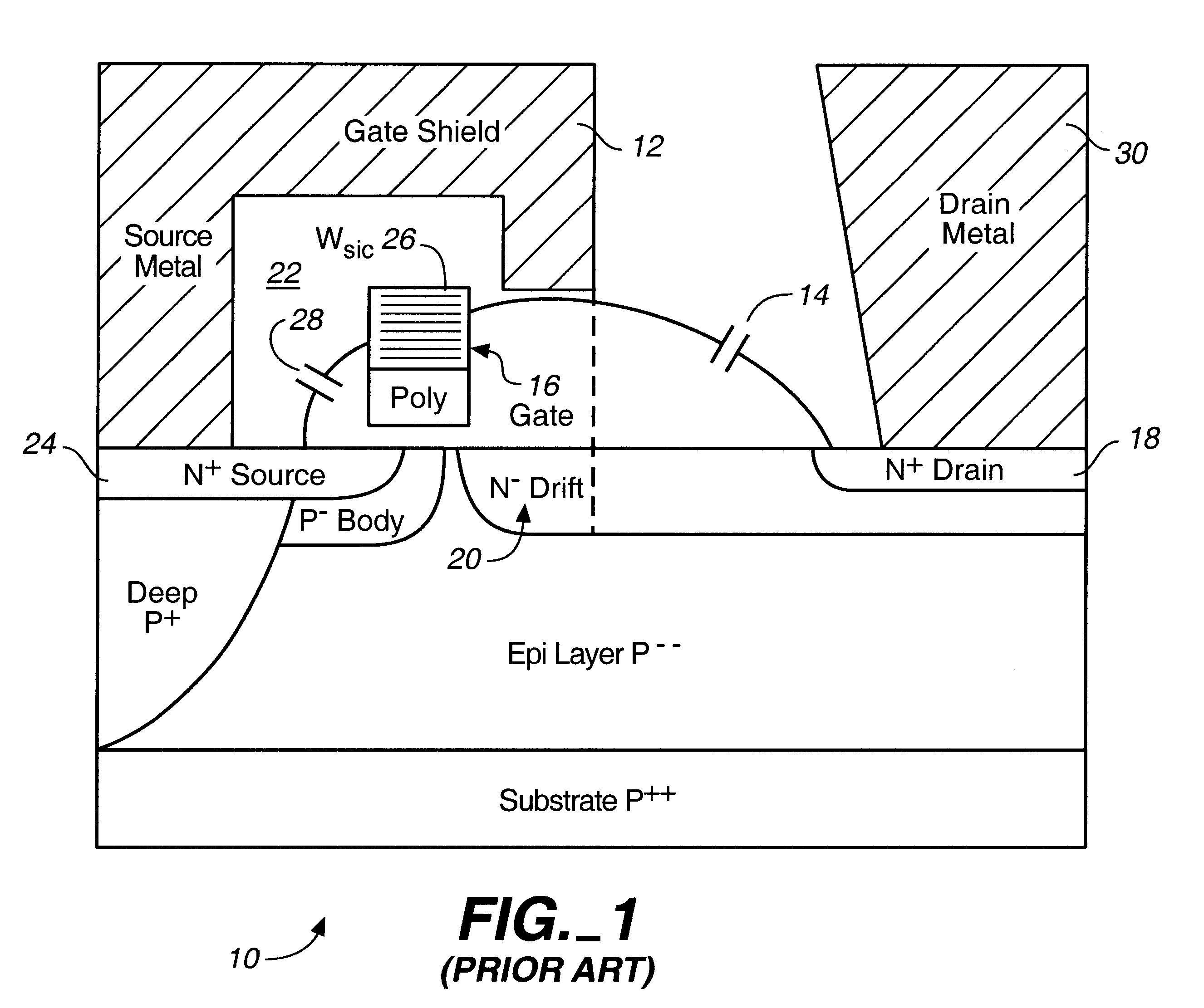
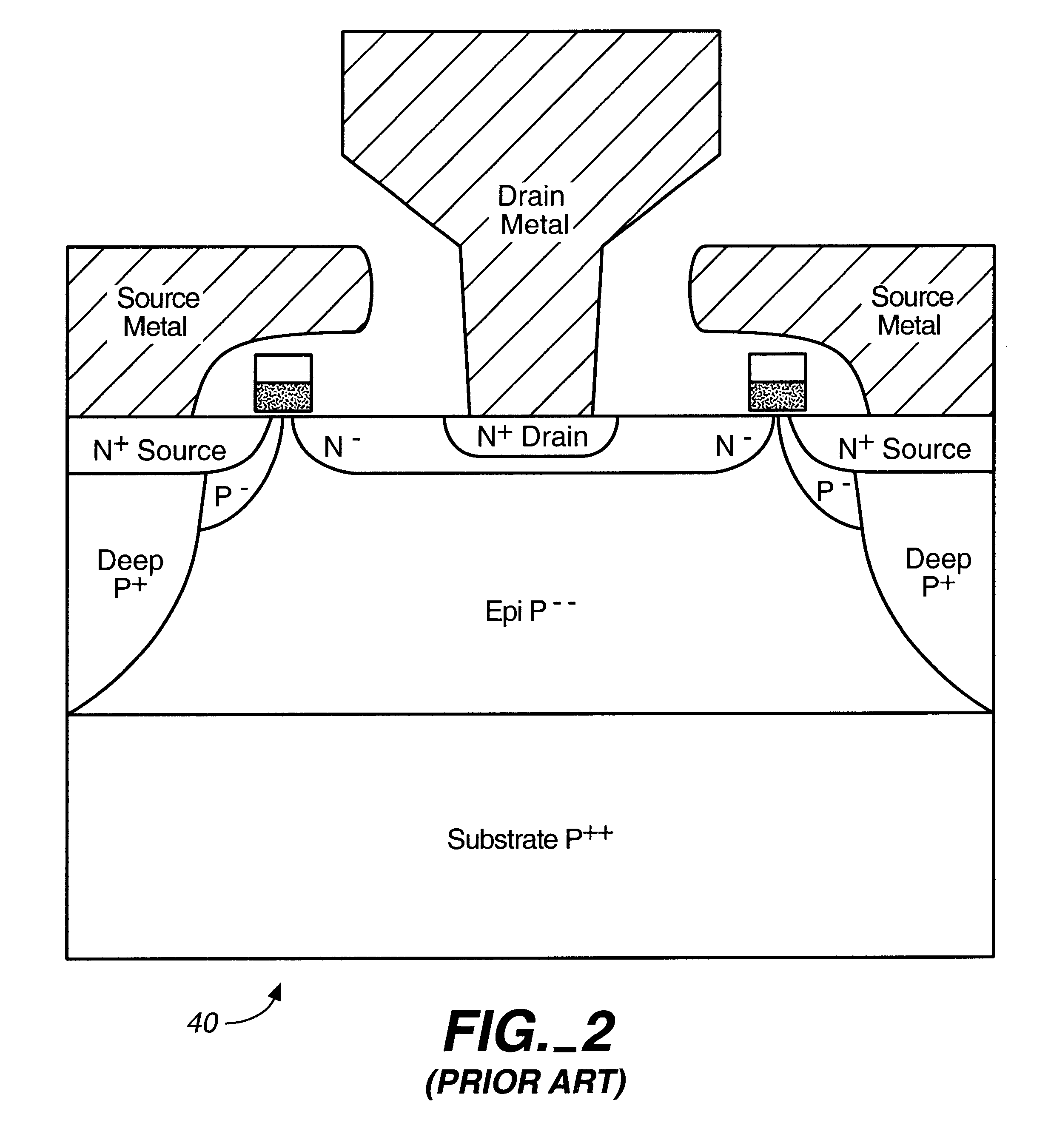
As processing technology improved, in the early 1970's a number of MOSFET vertical structures begun to challenge the dominance of the BJT at the lower RF frequencies, trading the cost of the large silicon area, necessary to provide the current capability in MOSFETs, for the cost of simple processing.
In fact, the question now is not how to obtain higher electrical performance out of Silicon FETs but since tighter and smaller geometries are being used to improve speeds of operation, the limitation that these devices built in Silicon experience is thermal dissipation.
Unfortunately, these efforts to utilize SiC material in the fabrication of devices for microwave power devices are hindered by technological problems associated with crystal growth, purity and doping; plus problems related to the development of suitable ohmic contacts and rectifying junctions.
Although rapid progress has been made recently in all these areas, growth and device fabrication technology is still primitive as compared to that of Silicon devices.
Unfortunately, the most commonly used dopants in Silicon Carbide require high activation energies as compared to Silicon and therefore for a given level of dopant, SiC has considerable less free electrons available and / or higher charge scattering, that is more resistivity.
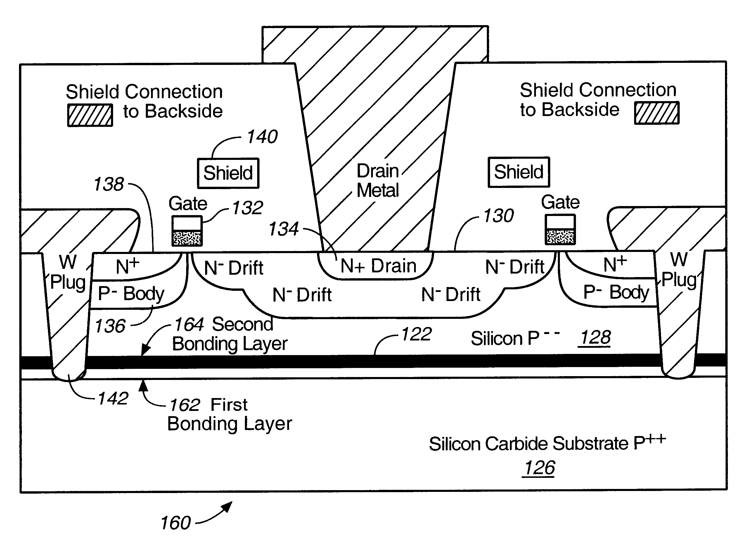
As the applications for wireless communications move up in the frequency spectrum, parasitic resistances, capacitances and inductances limit the performance of the multiple conductive plug structure for lateral RF MOS devices, as described in the '104 patent.

Method used


Image

  • Microwave field effect transistor structure on silicon carbide substrate
  • Microwave field effect transistor structure on silicon carbide substrate
  • Microwave field effect transistor structure on silicon carbide substrate

Examples


example i

Thermal Calculation

The thermal resistance calculations were made with formulations from Howes M. J., and Morgan D. V. "Reliability and Degradation", John Willey & Sons, Bath, England, 1981, page 422 The following structure (as shown in FIG. 9) was used for the computations.

From Howes and Morgan. For a square structure where T / W<2 the thermal resistances can be approximated as:

Rth=t(k.multidot.W) (0.25.multidot.t2+t+1); (Eq. 1)

where: t=T / W.

The Eq. 1 applied to the given above structure yielded the following results for the thermal resistances Rth (as shown in Table I):

The main cause of failure of RF power devices, when operated at high temperatures and current densities, is an electromigration failure in the topside metal layer. Since the failure rate of high power microwave devices is directly related to operating temperature, by utilizing Si-on-SiC (Si2C) technology the thermal resistance of the die structure can be considerably reduced, and therefore the operating life of devices ...

example ii

Electromigration Calculation

The MTF for an interdigitated LDMOS device due to metal electromigration in the drain fingers is calculated using The classical formula developed by Black from experimental results in the late '60s.

MTF=w t e (.theta. / KT) / C J2; (Eq. 2)

Wherein: w=line width; t=line thickness; .theta.=Activation energy;

K=Boltzman constant; T=temperature in oK; C=Material constant;

J=Current density

The main uncertainty in determining the MTF for a device is in using appropriate values for the activation energy .theta. of the metal layer used. Xemod's foundries use a metal sandwich of Al / 2%Cu / 1%Si, 1.5 microns thick, with and activation energy of between 0.93 eV and 0.65 eV depending on the width of the line in question. Replacing the dimensional values of the drain finger (the portion of the die topside metal with the highest current density) for a typical

XeMOS II structure into equation 1 we obtain:

MTF:=226 years for Silicon

MTF:=3086 years for Si2C

This lifetime was calculated...


PUM


Abstract

A microwave transistor structure comprising: (a) a SiC substrate having a top surface; (b) a silicon semiconductor material of a first conductivity type overlaying the top surface of the semiconductor substrate and having a top surface; (c) a conductive gate overlying and insulated from the top surface of the silicon semiconductor material; (d) a channel region of the first conductivity type formed completely within the silicon semiconductor material including a channel dopant concentration; (e) a drain region of the second conductivity type formed in the silicon semiconductor material and contacting the channel region; (f) a body region of the first conductivity type and having a body region dopant concentration formed in the silicon semiconductor material under the conductive gate region; (g) a source region of the second conductivity type and having a source region dopant concentration formed in the silicon semiconductor material within the body region; (h) a shield plate region being adjacent and being parallel to the drain region formed on the top surface of the silicon semiconductor material over a portion of the channel region; wherein the shield plate region is adjacent and parallel to the conductive gate region; and wherein the shield plate extends above the top surface of the silicon semiconductor material to a shield plate height level, and is insulated from the top-surface of the silicon semiconductor material; and (i) a conductive plug region formed in the body region of the silicon semiconductor material to connect a lateral surface of the body region to the top surface of the substrate.

Description

The present invention is in the field of microwave field effect transistors, and more specifically, is in the field of microwave power devices and integrated circuits that combines a lateral LDMOS structure to a composite material substrate technology.DISCUSSION OF THE PRIOR ARTIn the prior art, power high frequency devices have been built using a variety of semiconductor technologies. For a long time the preferred vehicle for their realization has been the NPN bipolar junction transistor (BJT). Its primary advantage was the achievable high intrinsic transconductance (gm) that permitted the fabrication of high power devices utilizing small silicon areas.As processing technology improved, in the early 1970's a number of MOSFET vertical structures begun to challenge the dominance of the BJT at the lower RF frequencies, trading the cost of the large silicon area, necessary to provide the current capability in MOSFETs, for the cost of simple processing. The advantages that the MOSFET st...

Claims


Application Information

Patent Timeline
Patent Type & Authority Patents(United States)
IPC IPC(8): H01L29/78H01L21/70H01L21/74H01L29/66H01L23/552H01L29/40H01L29/417H01L29/08H01L29/02H01L29/06H01L29/24
CPCH01L21/743H01L23/552H01L29/4175H01L29/41766H01L29/7835H01L29/0847H01L29/1608H01L29/402H01L2924/0002H01L2924/00
Inventor D'ANNA, PABLOJOHNSON, JOSEPH H.
Owner QORVO US INC
Learn More