Method of manufacturing array substrate

a manufacturing method and array substrate technology, applied in the direction of instruments, semiconductor devices, electrical equipment, etc., can solve the problems of reducing design freedom, reducing productivity, and restricting the design of gate wiring patterns

Inactive Publication Date: 2003-03-04
KK TOSHIBA
View PDF13 Cites 116 Cited by
  • Summary
  • Abstract
  • Description
  • Claims
  • Application Information

AI Technical Summary

Benefits of technology

Due to this multi-layer formation by an Al alloy layer and a refractory metal layer, no deformation of the Al layer and no failure of the dielectric film take place without causing decrease in the production yield of the array substrates. Thus, a wiring resistivity same or lower than that of prior art can be accomplished without causing decrease in the production yield.

Problems solved by technology

However, because anodic-oxidized films have to cover the surface of the aluminum wiring that is a low-resistivity wiring, the manufacturing method requires an anodic oxidation processing including a mask-forming process, and requires extra wiring patterns for voltage supply for the anodic oxidation processes.
Thus, a restriction arises in designing of gate wiring patterns, which are wiring patterns for scanning lines and gate electrodes.
This restriction leads to lower productivity and lower freedom in designing.
However, in this wiring pattern, deformation such as a hillock may occur.
Forming of the hillock on the wiring leads to deterioration of interlayer dielectric property of dielectric films, remarkably decreasing production yield of the array substrate.
Moreover, there has been a problem in that, at an etching process for forming pixel electrodes, its etchant penetrates into the Al wiring layer to corrode the Al, so as to lower the production yield.

Method used


Image

  • Method of manufacturing array substrate
  • Method of manufacturing array substrate
  • Method of manufacturing array substrate

Examples


Embodiment Construction

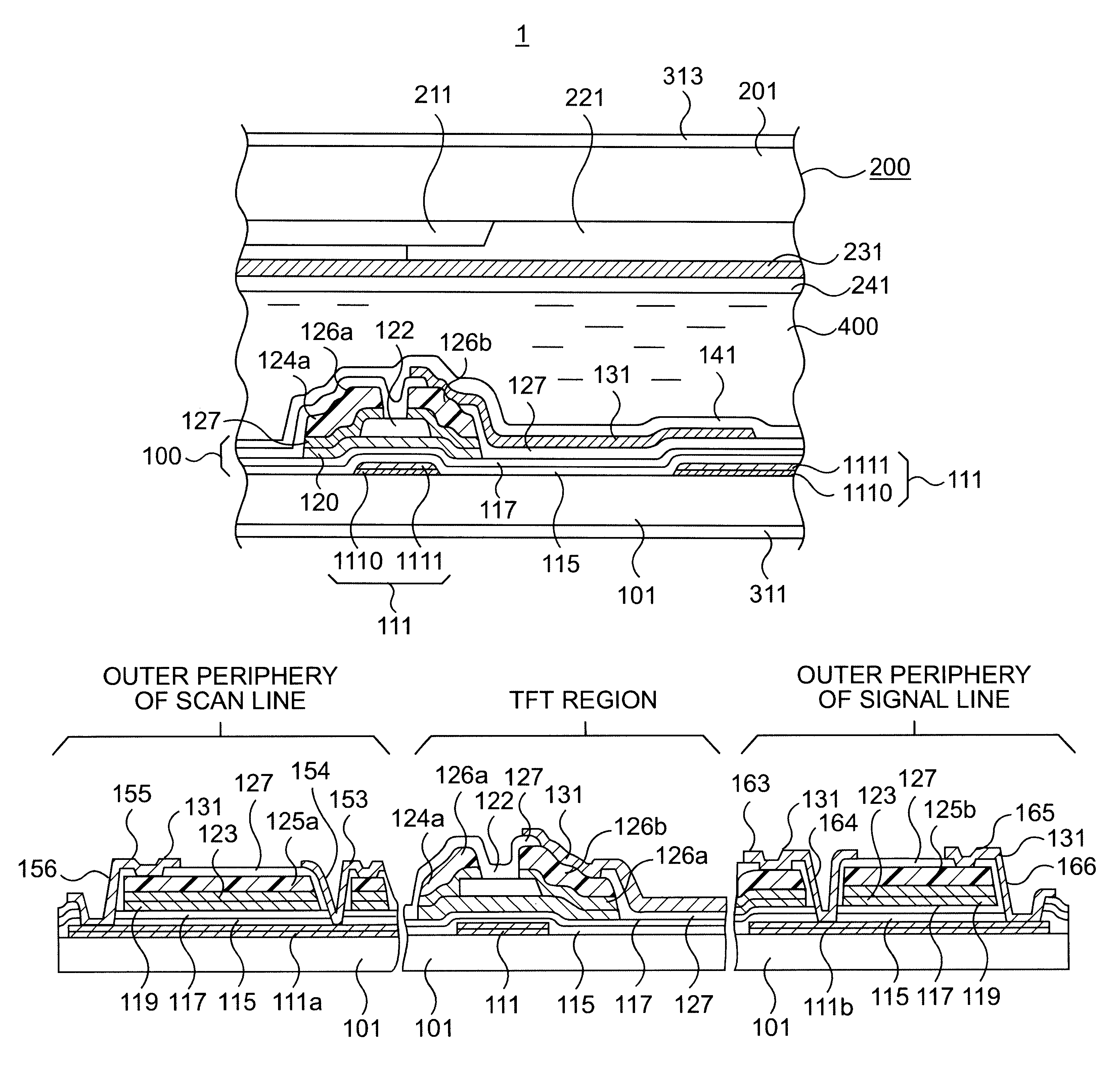
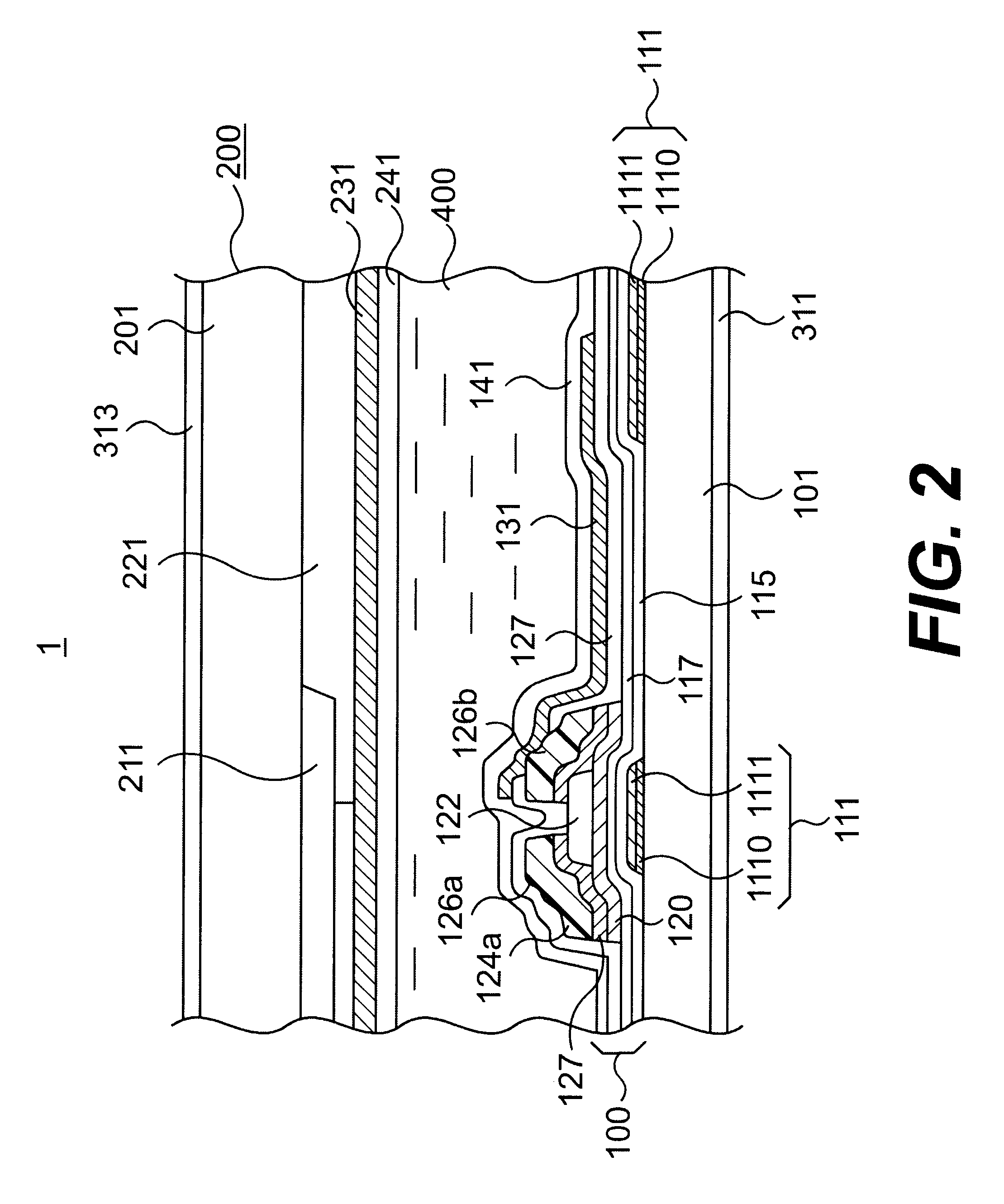
A description will now be given of a liquid crystal display (LCD) device 1 in accordance with an embodiment of the present invention with reference to FIGS. 1 through 13.

This LCD device 1 is of the light transmissive type capable of displaying color images. As shown in FIG. 2, LCD device 1 has an array substrate 100, an counter substrate 200, and a twisted nematic (TN) liquid crystal held therebetween through orientation films 141, 241 being laid between it and substrates 100,200. These orientation films 141, 241 are made of polyimide resin. Also, polarization plates 311, 313 are adhered to the outer surfaces of array substrate 100 and counter substrate 200, respectively.

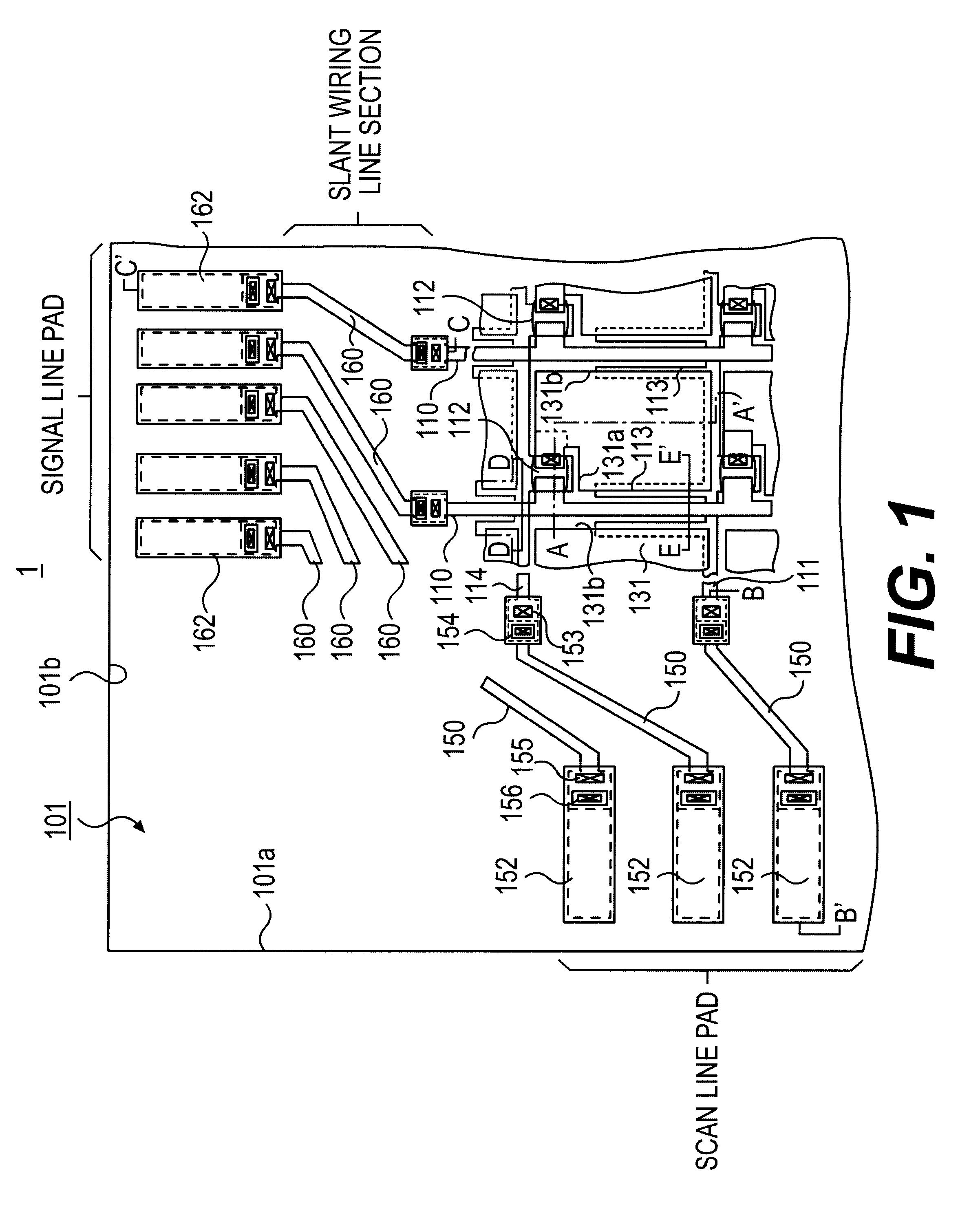
FIG. 1 shows a schematical plan view of the array substrate 100, wherein the lower side of this drawing is to be located at the upper side of the display screen of LCD device 1 while allowing scanning lines to be successively selected in the sequence from the lower to the upper side of the illustration.

The array sub...


PUM


Abstract

In the manufacturing method of array substrates for use in flat panel display devices including liquid crystal display (LCD) devices, it is aimed to prevent failure of interlayer dielectric film due to wiring deformation or the like while reducing the resistivity of wiring. It is also aimed to prevent corrosion of a metal wiring layer at the etching process and to thereby prevent deterioration of production yield due to corrosion. According to the method of the invention, to form scanning lines (111), an aluminum-neodymium alloy (Al-Nd) film (1110) is deposited in 300 nm thickness on the first hand, and then 50 nm thick Mo film (1110) is deposited thereon. Subsequently, gate insulator films (115 and 117) are formed by CVD processes at a substrate temperature of 350° C. Further, an etching process for forming pixel electrode (131) is carried out by HBr, HI, Oxalic acid or a mixture liquid containing at least one of these acids.

Description

1. Field of the InventionThe present invention relates to the manufacturing method of array substrates for use in flat panel display devices including liquid crystal display (LCD) devices.2. Description of the Related ArtIn the recent years flat panel display devices are more frequently developed to replace conventional cathode-ray tube (CRT) units; in particular, LCD devices are becoming commercially attractive more and more due to their advantage such as light weight, thinness, low power consumption and the like.As one typical prior known LCD devices, a light transmissive active-matrix LCD device will now be described herein which comes with a plurality of switch elements each of which is at a respective one of picture elements. The active-matrix LCD device includes a liquid crystal layer held between an array substrate and a counter substrate with orientation films being provided between the liquid crystal layer and any one of such substrates. The array substrate has, on a transp...

Claims


Application Information

Patent Timeline
Patent Type & Authority Patents(United States)
IPC IPC(8): H01L21/02H01L27/12H01L21/70H01L21/336H01L29/45H01L29/40H01L29/49H01L21/84H01L21/77
CPCH01L27/1214H01L29/66765H01L29/4908H01L29/458H01L27/124H01L27/1259G02F1/1343G02F1/136
Inventor DOJO, MASAYUKIKUBO, AKIRA
Owner KK TOSHIBA
Why Eureka
Try Eureka