Method of fabricating a nickel/platinum monsilicide film

a nickel-platinum monosilicide and film technology, applied in the direction of basic electric elements, electrical equipment, semiconductor devices, etc., can solve the problems of high sheet resistance and substantial drawbacks of titanium silicide layers (titanium disilicides) when using narrow line widths, and achieve low leakage current, high solubility of silicon, and diffuse very quickly

Inactive Publication Date: 2003-03-11
AGENCY FOR SCI TECH & RES
View PDF3 Cites 48 Cited by
  • Summary
  • Abstract
  • Description
  • Claims
  • Application Information

AI Technical Summary

Benefits of technology

It is an object of the present inventions to provide a method of fabricating a nickel-platinum monosilicide on a silicon semiconductor whilst controlling the formation of nickel and platinum related defects to an acceptable level.
It is a further object of the present invention to provide a method of fabricating a nickel-platinum monosilicide on a semiconductor structure to produce a semiconductor device having a low leakage current.
The primary aim of the present invention is to minimise the formation of electrically active defects within a semiconductor device caused by the formation of a nickel-platinum monosilicide layer on a silicon wafer.
It has been found that by controlling the annealing step such that annealing takes place at a critical temperature range of between 680.degree. C. and 720.degree. C., the formation of electrically active defects can be minimised and reduced to an acceptable level. The acceptable level for the formation of nickel related defects and platinum related defects estimated from the SIA Road Map ("National Technology Road Map for Semiconductors", Semiconductor Industry Association 1997) are below 1.times.10.sup.14 defects / cm.sup.3 and 2.times.10.sup.13 defects / cm.sup.3 respectively. An annealing temperature range of between 690.degree. C. and 710.degree. C. is preferred. Typically, the annealing process will take in the region of 10 to 60 seconds and it is necessary to control the annealing temperature within the above indicated range during this period.

Problems solved by technology

The resultant titanium silicide layer (titanium disilicide) has a substantial drawback.
That drawback is the high sheet resistance encountered when using narrow line widths.

Method used


Image

  • Method of fabricating a nickel/platinum monsilicide film
  • Method of fabricating a nickel/platinum monsilicide film
  • Method of fabricating a nickel/platinum monsilicide film

Examples


Embodiment Construction

Referring to FIG. 3, a silicon semiconductor structure 1 comprises, inter alia, a surface having silicon regions 2 (i.e. source / drain regions) and adjacent insulating regions 3. Turning now to FIG. 4, a layer comprising nickel and platinum is deposited as a blanket film 4 over the silicon regions 2 and the adjacent insulating regions 3 of the silicon semiconductor structure, using a conventional deposition process. The resultant nickel / platinum layer 4 has a 95% nickel content and a 5% platinum content. The film 4 may include other elements such as, for example, titanium.

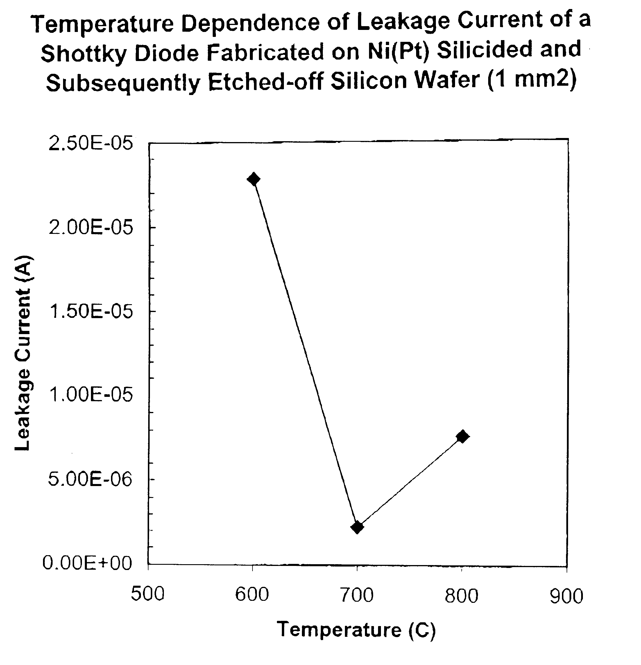
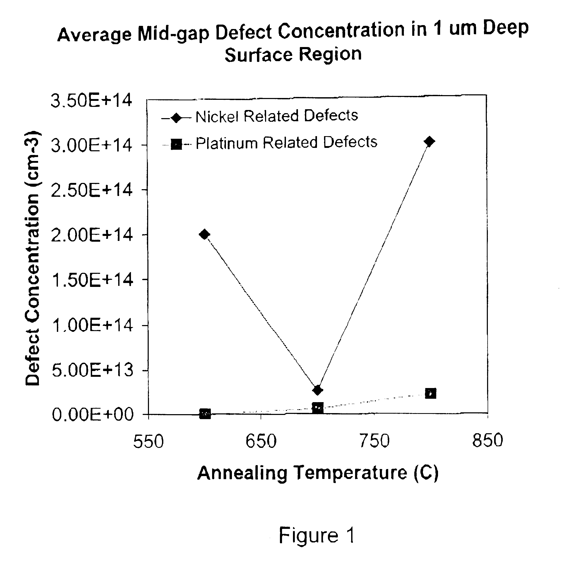
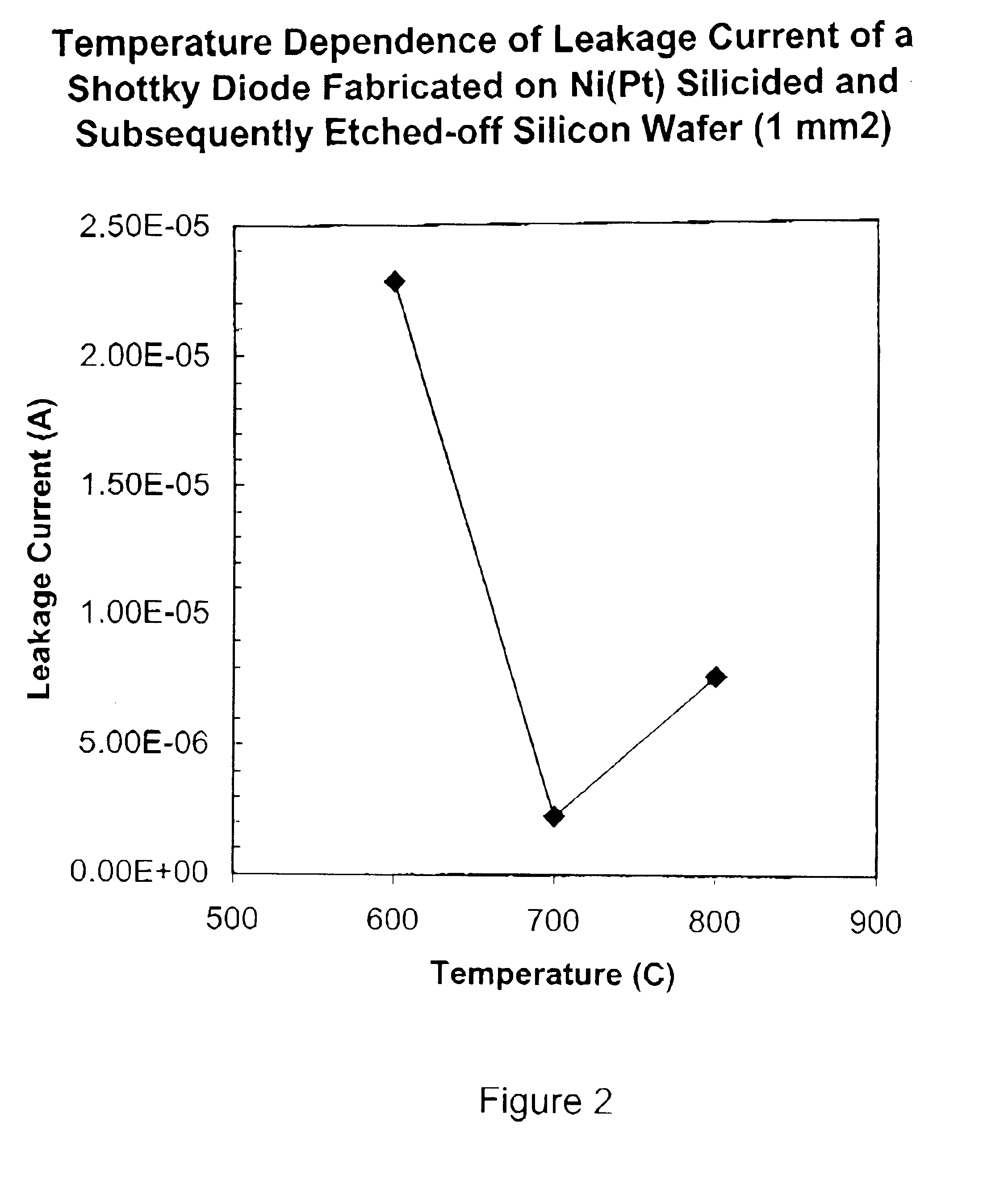
The silicon semiconductor structure 1 and the nickel / platinum layer 4 are then subjected to high temperature rapid thermal annealing to form a nickel-platinum monosilicide 5 on the silicon regions 2 as shown in FIG. 5. The annealing takes place in a nitrogen atmosphere at a temperature of 700.degree. C. The annealing process takes 60 seconds.

After annealing, any excess nickel / platinum film 4 on top of the insulating...


PUM


Abstract

A method of fabricating a silicide layer on a silicon region of a semiconductor structure, the method comprising the steps of: providing a semiconductor structure having at least one silicon region on a surface thereof; depositing a layer comprising nickel and platinum on the at least one silicon layer; annealing the semiconductor structure and the nickel / platinum layer to react the nickel and the platinum with underlying silicon to form a nickel-platinum silicide, wherein annealing step takes place at temperature of between 680° C. and 720° C.

Description

THIS INVENTION relates to a method of fabricating semiconductor structures and more particularly to a method of forming nickel-platinum monosilicide on a silicon semiconductor device.Silicide processes are used in the manufacture of large-scale integrated silicon circuit devices to provide a silicide layer with low sheet resistance on a silicon semiconductor structure or device.Typically, the surface of a silicon semiconductor or device is adjoined by regions of silicon and regions of insulating materials like silicon oxide, silicon nitride, silicon oxynitride and aluminium oxide. A film is deposited on the surface of the silicon semiconductor structure or device using conventional deposition techniques such as sputtering, electron-beam evaporation, or filament evaporation. The film can be deposited by sputtering an alloy target or by co-sputtering two or more pure targets. Once the film has been deposited on the silicon layer, the semiconductor device is annealed using a rapid ther...

Claims


Application Information

Patent Timeline
IPC IPC(8): H01L21/336H01L21/02H01L29/40H01L29/49
CPCH01L21/28518H01L29/665H01L29/4933
Inventor CHI, DONGZHILAHIRI, SYAMAL KUMARMANGELINCK, DOMINIQUE
Owner AGENCY FOR SCI TECH & RES
Why Eureka
Try Eureka