Metal-oxide electron tunneling device for solar energy conversion

a technology of electron tunneling and solar energy, which is applied in the direction of pv power plants, light radiation electric generators, generators/motors, etc., can solve the problems of high energy conversion efficiency of semiconductor solar cells, inability to provide the amount of power, and inability to achieve the ratio of incident solar power to electrical power ou

Inactive Publication Date: 2003-03-18
UNIV TECH
View PDF1 Cites 181 Cited by
  • Summary
  • Abstract
  • Description
  • Claims
  • Application Information

AI Technical Summary

Benefits of technology

As will be seen hereinafter, the present invention provides a significant improvement over the prior art as discussed above by virtue of its ability to provide the increased performance while, at the same time, having significant advantages in its manufacturability. This assertion is true for electromagnetic devices generally, which take advantage of the present invention, as well as solar energy conversion devices in particular.
, as well as solar energy conversion devices in particular.
1. J. G. Simmons, "Electric tunnel effect between dissimilar electrodes separated by a thin insulating film," Journal of Applied Physics, 34 (1963).
2. S. R. Pollack and C. E. Morris, "Electron tunneling through asymmetric films of thermally grown Al.sub.2 O.sub.3," Journal of Applied Physics, vol. 35, no. 5 (1964).
3. L. O. Hocker, et al., "Frequency mixing in the infrared and far-infrared using a metal-to-metal point contact diode," Applied Physics Letters, vol. 12, no. 12 (1968).
4. S. M. Faris, et al., "Detection of optical and infrared radiation with DC-biased electron-tunneling metal-barrier-metal diodes," IEEE Journal of Quantum Electronics, vol. QE-9, no. 7 (1973).

Problems solved by technology

Recent energy crises have highlighted the growing demands placed on traditional sources of power, such as gas and electricity.
One of the main obstacles preventing the proliferation of solar energy conversion systems is efficiency.
Currently available semiconductor solar cell systems are not able to provide the amount of power for the dollar that is possible by traditional power sources.
Especially semiconductor solar cells with high energy conversion efficiency (ratio of incident solar power to electrical power out) are expensive.
Most solar cell systems are based on semiconductor technology, which can be difficult to scale to the size required for large solar panels.
Using the present technology, it is expensive to fabricate a semiconductor-based solar panel which is large enough to replace the traditional sources of power.
In other words, the response of the semiconductor device is limited by the bandgap energy.
Thus, the semiconductor device does not respond at all to photons having energy less than the bandgap energy, and incident electromagnetic energy in excess of the bandgap energy is wasted in the energy conversion.
Currently available MIM devices are not able to provide sufficiently high degrees of asymmetry and nonlinearity with sufficiently low differential resistance in the current-to-voltage performance, hence the energy conversion efficiency of MIM devices is low.
However, the MIMIMIM devices of Suemasu and Asada have the distinct disadvantage of being a much more complicated device than the simple MIM device.
Therefore, although the goal of increased nonlinearity and asymmetry may be achieved in the MIMIMIM devices of Suemasu and Asada using metal and insulator combinations, the simplicity of the MIM structure is lost.
Current crystal growth techniques theoretically enable the implementation of the SIIS structure, but an SIIS device would still embody the drawbacks inherent in semiconductor materials, namely cost efficiency in large area devices.
In addition, Suemasu (see Ref. 7) speculates that the recent trend of decreasing the size of electronic devices in order to achieve high speed switching will make semiconductor-based devices impractical due to fluctuation of carrier concentration, which occurs when semiconductor devices are reduced to mesoscopic regimes.

Method used


Image

  • Metal-oxide electron tunneling device for solar energy conversion
  • Metal-oxide electron tunneling device for solar energy conversion
  • Metal-oxide electron tunneling device for solar energy conversion

Examples


Embodiment Construction

The following description is presented to enable one of ordinary skill in the art to make and use the invention and is provided in the context of a patent application and its requirements. Various modifications to the described embodiments will be readily apparent to those skilled in the art and the generic principles herein may be applied to other embodiments. Thus, the present invention is not intended to be limited to the embodiment shown but is to be accorded the widest scope consistent with the principles and features described herein.

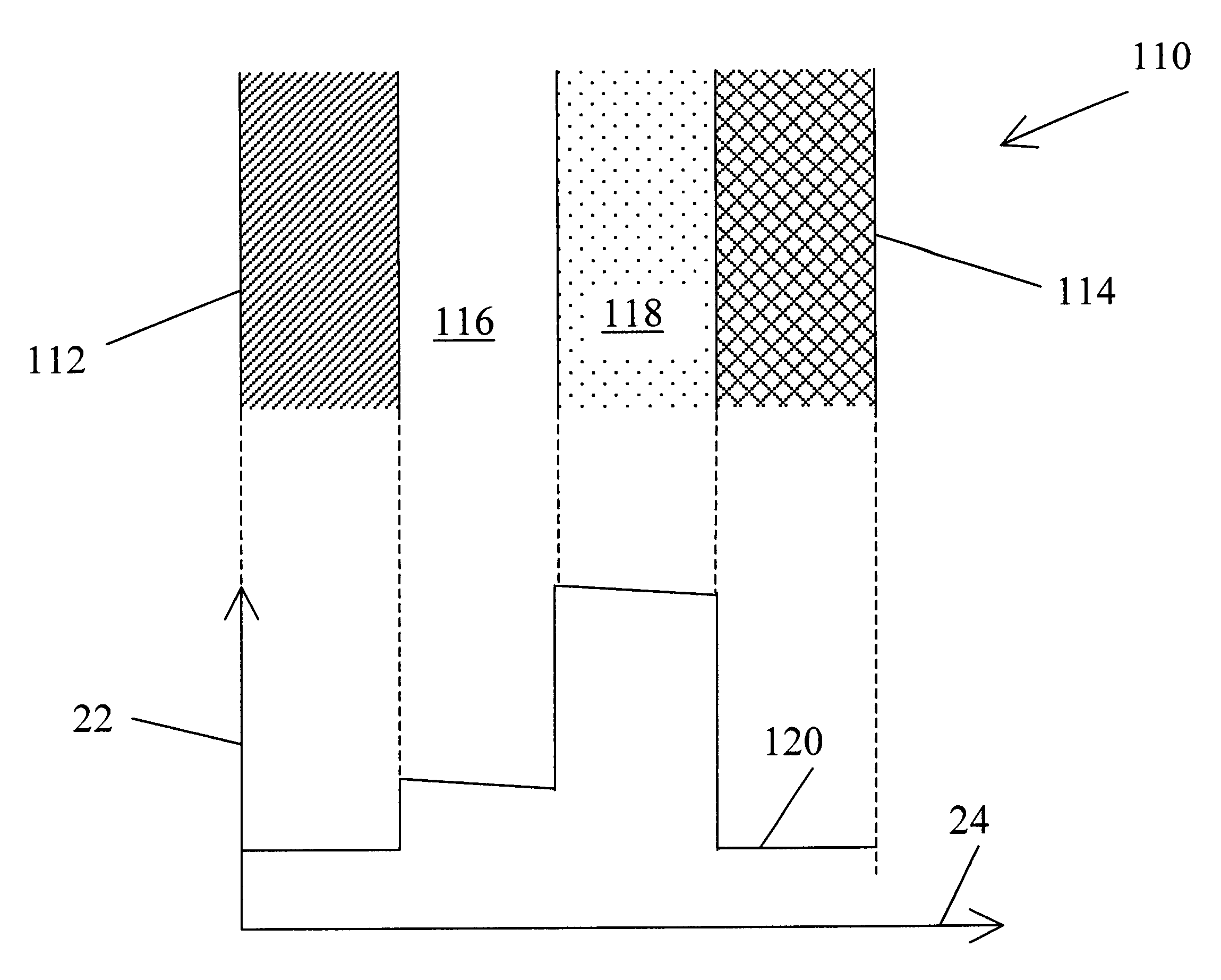
Referring now to FIG. 2A, an electron tunneling device designed in accordance with the present invention is described. The electron tunneling device, generally indicated by reference number 110, includes a first non-insulating layer 112 and a second non-insulating layer 114. Non-insulating materials include, for example, metals, superconductors, semiconductors, semimetals, quantum wells and superlattice structures. First non-insulating layer 112 a...


PUM


Abstract

The electron tunneling device includes first and second non-insulating layers spaced apart such that a given voltage can be provided therebetween. The device also includes an arrangement disposed between the non-insulating layers and configured to serve as a transport of electrons between the non-insulating layers. This arrangement includes a first layer of an amorphous material such that using only the first layer of amorphous material in the arrangement would result in a given value of a parameter in the transport of electrons, with respect to the given voltage. The arrangement further includes a second layer of material, which is configured to cooperate with the first layer of amorphous material such that the transport of electrons includes, at least in part, transport by tunneling, and such that the parameter, with respect to the given voltage, is increased above the given value of the parameter.

Description

BACKGROUND OF THE INVENTIONThe present invention relates generally to optoelectronic devices and, more particularly, to electron tunneling devices, especially for solar energy conversion.Recent energy crises have highlighted the growing demands placed on traditional sources of power, such as gas and electricity. With rising energy costs, it is desirable to find alternative power sources to augment traditional power sources such as hydroelectric and thermonuclear. Solar energy conversion provides such an alternative by tapping into the readily available power of the sun.One of the main obstacles preventing the proliferation of solar energy conversion systems is efficiency. Currently available semiconductor solar cell systems are not able to provide the amount of power for the dollar that is possible by traditional power sources. Especially semiconductor solar cells with high energy conversion efficiency (ratio of incident solar power to electrical power out) are expensive. Most solar...

Claims


Application Information

Patent Timeline
Patent Type & Authority Patents(United States)
IPC IPC(8): G02B6/26H01L21/00H01L31/102H01L25/00H01L29/02H01L29/06H01L31/0328H01L31/06H02N6/00H01L31/0264H01L31/072H01L31/09H01L31/0336H01L31/08H01L31/04H01L31/109H01L31/101H01L45/00
CPCB82Y20/00H01L31/035236H01L31/101H01L45/00H01L31/06Y02E10/50H10N70/00H02S10/00
Inventor ELIASSON, BLAKE J.MODDEL, GARRET
Owner UNIV TECH
Why Eureka
Try Eureka