Electron device and semiconductor device

a technology of electromagnetic devices and semiconductors, applied in the directions of hermetically sealed casings, electrical apparatus casings/cabinets/drawers, and semiconductor/solid-state device details, etc., can solve problems such as damage to parts

Inactive Publication Date: 2003-04-29
HITACHI LTD
View PDF12 Cites 41 Cited by
  • Summary
  • Abstract
  • Description
  • Claims
  • Application Information

AI Technical Summary

Benefits of technology

Another object of the present invention is to improve reliability of a solder joint in a semiconductor device die-bonded Si chip or the like to which thermal shock causing large deformation may act, bump mounting of BGA, CSP, WPP, flip-chip and so forth, a power module acting large stress and so forth.
More particularly, by employing a material easy to deform and superior to elongate than Sn--Ag--Cu type solder when impulsive large force act on the solder, stress load in the joint interface of the parts can be eliminated without degrading reliability in heat cycle of the joint to improve falling down resistance and impact resistance to improve thermal shock absorbing function for large deformation. Namely, as Pb free solder of Sn base used in the joint portion, a material having small stress and material easy to deform is prepared by solving In which is softer than Sn in the matrix of Sn or Sn--Cu to improve falling down resistance and impact resistance by absorbing impact to be exerted on the joint interface as falling down.
By this, impact energy upon falling down is absorbed by plastic deformation of the solder per se to reduce stress to be exerted on the joint interface. Therefore, large impact force will not act on the joint interface to improve impact resistance.
On the other hand, even in solder bump connection of the semiconductor device die-bonded the Si-chip or the like, mounting of BGA, CSP, WPP (Wafer Process Package), flip-chip and connection of large area power module to which large stress act, upon soldering causing large deformation and upon thermal shock acceleration test or the like, breakage due to stress concentration at the interface is prevented and reliability of connection can be achieved by employing a material having low strength and easy to deform.

Problems solved by technology

However, in contrast to this, when parts, printed circuit board and so forth is low in strength, since solder per se is not broken, stress concentration is caused at joint interface to possibly damage the parts or the like.

Method used


Image

  • Electron device and semiconductor device
  • Electron device and semiconductor device
  • Electron device and semiconductor device

Examples


Embodiment Construction

The present invention will be discussed hereinafter in detail in terms of the preferred embodiment of the present invention with reference to the accompanying drawings. In the following description, numerous specific details are set forth in order to provide a thorough understanding of the present invention. It will be obvious, however, to those skilled in the art that the present invention may be practiced without these specific details. In other instance, well-known structure are not shown in detail in order to avoid unnecessary obscurity of the present invention.

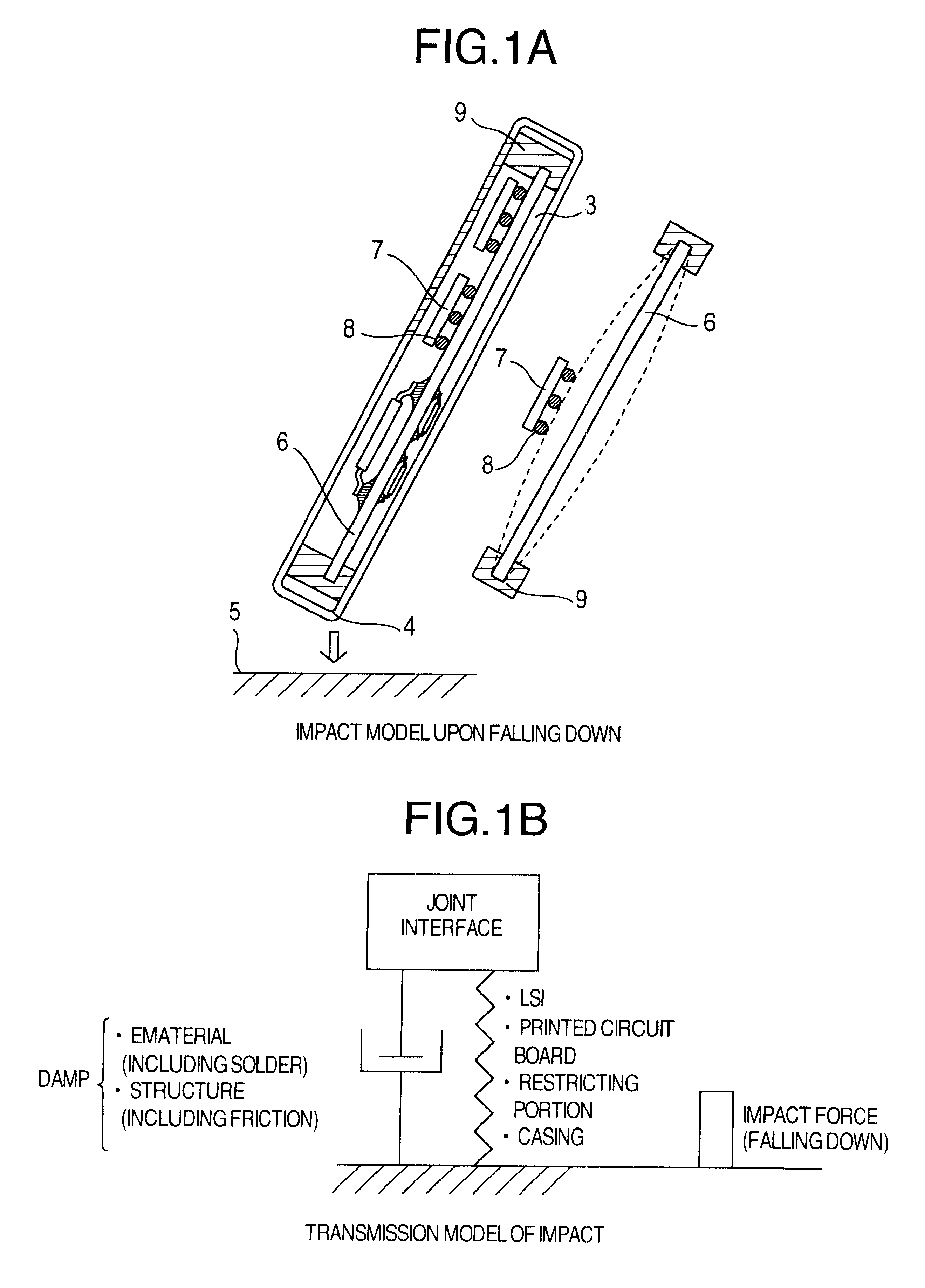
At first, discussion will given for impact for the case where an electronic equipment, such as a cellular telephone or the like is fallen down.

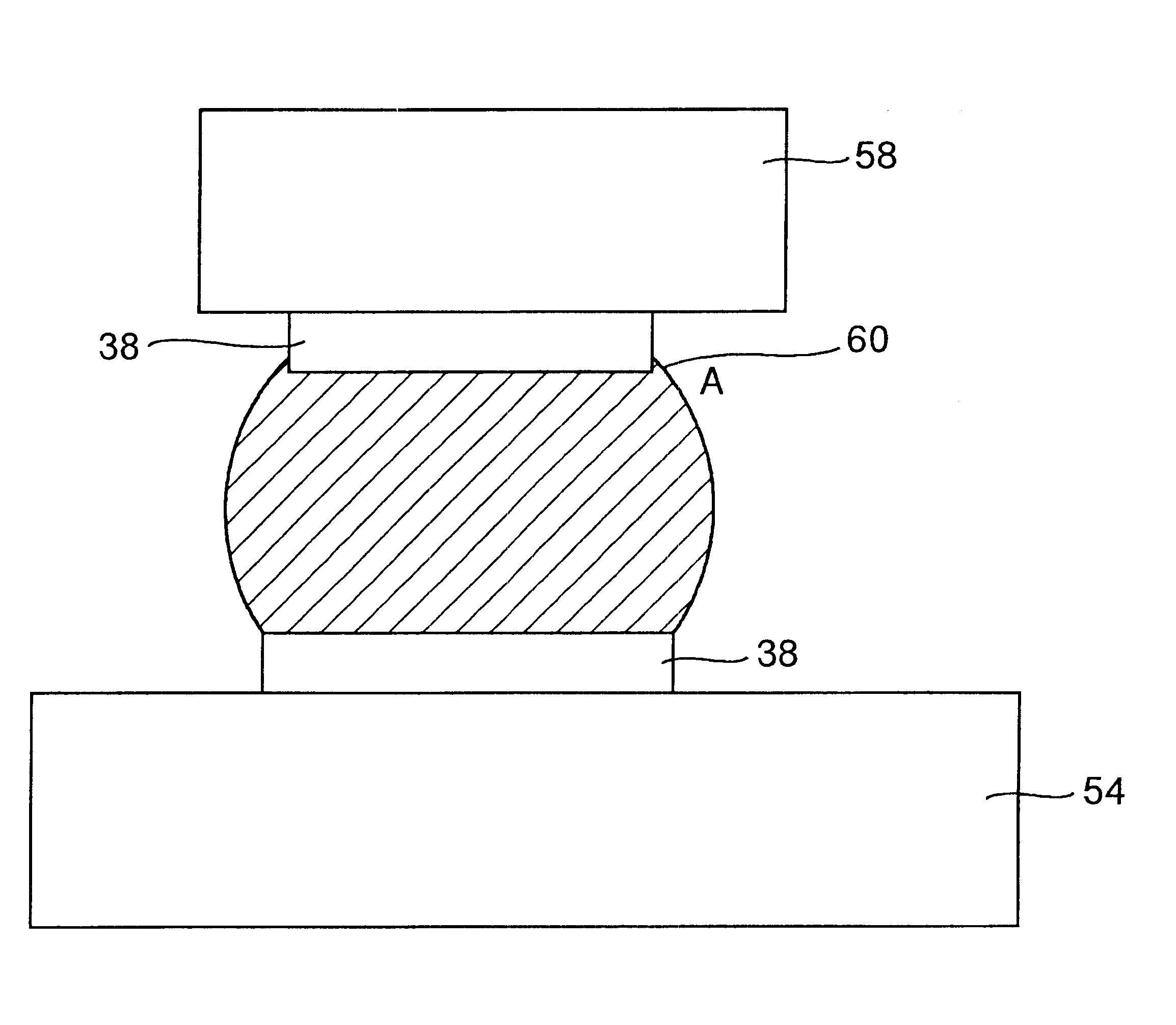
In a casing of the electronic equipment, such as a cellular telephone or the like, various parts, LSIs (packages of BGA, CSP, TSOP, TQFP and so on) are mounted on a printed circuit board. Such parts and LSIs rarely damaged by normal falling down. However, falling down from high pos...


PUM

PropertyMeasurementUnit
elongationaaaaaaaaaa
melting pointaaaaaaaaaa
weightaaaaaaaaaa

Abstract

An electronic equipment is capable of improving falling down shock resistance or impact resistance in an electronic equipment and of improving reliability of a solder joint in a semiconductor device die-bonded Si chip or the like to which thermal shock causing large deformation may act, bump mounting of BGA, CSP, WPP, flip-chip and so forth, a power module acting large stress and so forth. The electronic equipment has a circuit board and an electronic parts to be electrically connected to an electrode of the circuit board. The electrode of the circuit board and an electrode of the electronic part are connected by soldering using a lead free solder consisted of Cu: 0~2.0 mass %, In: 0.1~10 mass %, and Sn: remaining amount.

Description

1. Field of the InventionThe present invention relates to a technology applicable for an electronic equipment mounting electronic parts (particularly, a mobile product required high impact strength), a CSP package required resistance of thermal shock, a MCM (multi-chip module) as a semiconductor module, a semiconductor device die-bonded Si chip or the like, connection of a large area power module, and so forth.2. Description of the Related ArtCurrently, in viewpoint of environmental protection, use of Pb free soldering is promoted. It is a worldwide trend irrespective of kind of electronic equipments that solder is transiting from conventional Sn--Pb eutectic type solder to high temperature type solder of Sn--Ag--Cu type, such as Sn-(2.0.about.4.0)Ag-(0.5.about.1.5)Cu, which can expect high reliability of joint. In comparison with the conventional full universal type Sn--Pb eutectic type solder, Sn--Ag--Cu type solder has to pay attention for possibility of degradation of reliabilit...

Claims


Application Information

Patent Timeline
Patent Type & Authority Patents(United States)
IPC IPC(8): B23K35/26H01L21/60H01L21/02H05K3/34
CPCB23K35/262H01L24/32H01L24/33H01L24/81H05K3/3463B23K2201/36H01L2224/131H01L2224/13144H01L2224/1319H01L2224/16225H01L2224/16227H01L2224/32225H01L2224/32245H01L2224/48091H01L2224/48227H01L2224/48247H01L2224/73204H01L2224/73265H01L2224/81801H01L2924/01013H01L2924/01029H01L2924/01033H01L2924/01047H01L2924/01049H01L2924/0105H01L2924/01051H01L2924/01078H01L2924/01079H01L2924/01082H01L2924/01322H01L2924/01327H01L2924/10329H01L2924/15311H01L2924/16152H01L2924/20106H01L2924/0132H01L2924/0133H01L2924/00013H01L2924/01005H01L2924/01006H01L2924/01042H01L2924/01074H01L2924/01075H01L2924/014H01L2924/0134H01L2224/291H01L2924/15738H01L2924/1576H01L2224/293H01L2224/29109H01L2224/29111H01L2224/29299H01L2224/2929H01L2924/10253Y10T428/12528H01L2924/00014H01L2224/13099H01L2924/00012H01L2924/01026H01L2924/01028H01L2924/00H01L2924/3512H01L2224/29099H01L2224/29199B23K2101/36H01L24/05H01L24/73H01L2224/05155H01L2224/05568H01L2224/05573H01L2224/05644H01L2224/2612H01L2924/181H01L23/12
Inventor SOGA, TASAOSHIMOKAWA, HANAENAKATSUKA, TETSUYANAKAMURA, MASATOFUJITA, YUJIISHIDA, TOSHIHARUOKAMOTO, MASAHIDESERIZAWA, KOJIHACHIYA, TOSHIHIROMUKUNO, HIDEKI
Owner HITACHI LTD
Why Eureka
Try Eureka