Ferroelectric-type nonvolatile semiconductor memory and operation method thereof

a nonvolatile semiconductor and non-volatile technology, applied in the direction of transistors, solid-state devices, instruments, etc., can solve the problems of large area occupied by peripheral circuits, difficult layout of peripheral circuits, and difference in accumulated charge amount of capacitor members, etc., to achieve high integration and increase capacity

Inactive Publication Date: 2003-05-20
SONY CORP
View PDF8 Cites 50 Cited by
  • Summary
  • Abstract
  • Description
  • Claims
  • Application Information

AI Technical Summary

Benefits of technology

It is a first object of the present invention to provide a ferroelectric-type nonvolatile semiconductor memory that can be increased in capacity without being limited by the minimum fabrication dimension and is more highly integrated.
In the operation method according to the second aspect of the present invention, the data stored in the memory cells sharing the plate line in the memory units in the number of N is read out and the data is re-written into the memory cells sharing the plate line in the memory units in the number of N by performing the potential rising and potential falling of the plate line once each, so that the frequency of each memory cell suffering a disturbance can be decreased, and that the rapid operation and low power consumption can be attained. In the operation method according to the third aspect of the present invention, readout of the data stored in the memory cells sharing the plate line in the memory units in the number of N is performed by providing the plate line with a pulse and then consecutively selecting the transistors for selection in the number of N, so that the frequency of each memory cell suffering a disturbance can be decreased, and that the rapid operation and low power consumption can be attained.

Problems solved by technology

As a result, there is caused a difference in the accumulated charge amount in the capacitor member.
It is therefore difficult to layout peripheral circuits, and the area that the peripheral circuits occupy comes to be large.
Further, such micro-fabrication techniques are facing increasing difficulties generation after generation, and the amount of investments comes to be huge amounts of money, which results in an increase in a chip cost.
In the semiconductor memory, therefore, it is difficult to achieve break-through improvements in storage capacity at present for a short period of time.
However, no sufficient yield or performances have been attained.
Further, even if the above attempts can be successfully made, the number of steps increases approximately twice for manufacturing memory cell in the semiconductor crystal layer, which results in spoiling of a cost merit.
There is therefore caused another difficulty in the layout of the peripheral circuits.
As described above, the memory cells per se are limited to the two-dimensional layout, and further, even if the memory cells are decreased in size, the address selection method that can be employed at present causes a difficulty on the layout of the peripheral circuits.
Further, while the method of decreasing the area of the nonvolatile memory disclosed in JP-A-121032 / 1997 is very effective, it has the following problems.
Therefore, if no measures are taken against the characteristic that the inversion voltage of a ferroelectric material for constituting the ferroelectric layer has the above negative temperature characteristic, the operation of the nonvolatile memory in a temperature range required of LSI may be no longer ensured.
Further, when the nonvolatile memory having the above structure is more shrunk, it is inevitably required to decrease the area of the capacitor member.
Such a sense signal amount provides an insufficient sense margin, and when the nonvolatile memory is further shrunk, readout of data stored in the nonvolatile memory can be no longer performed.
However, the above-constituted nonvolatile memory has a problem that three transistors are required per memory cell, so that the cell area per bit greatly increases, and that the cost per bit increases.
As a result, no sufficient electric field is formed between the upper electrode and the lower electrode, which causes a problem that no polarization inversion takes place in the ferroelectric layer.

Method used


Image

  • Ferroelectric-type nonvolatile semiconductor memory and operation method thereof
  • Ferroelectric-type nonvolatile semiconductor memory and operation method thereof
  • Ferroelectric-type nonvolatile semiconductor memory and operation method thereof

Examples


example 1

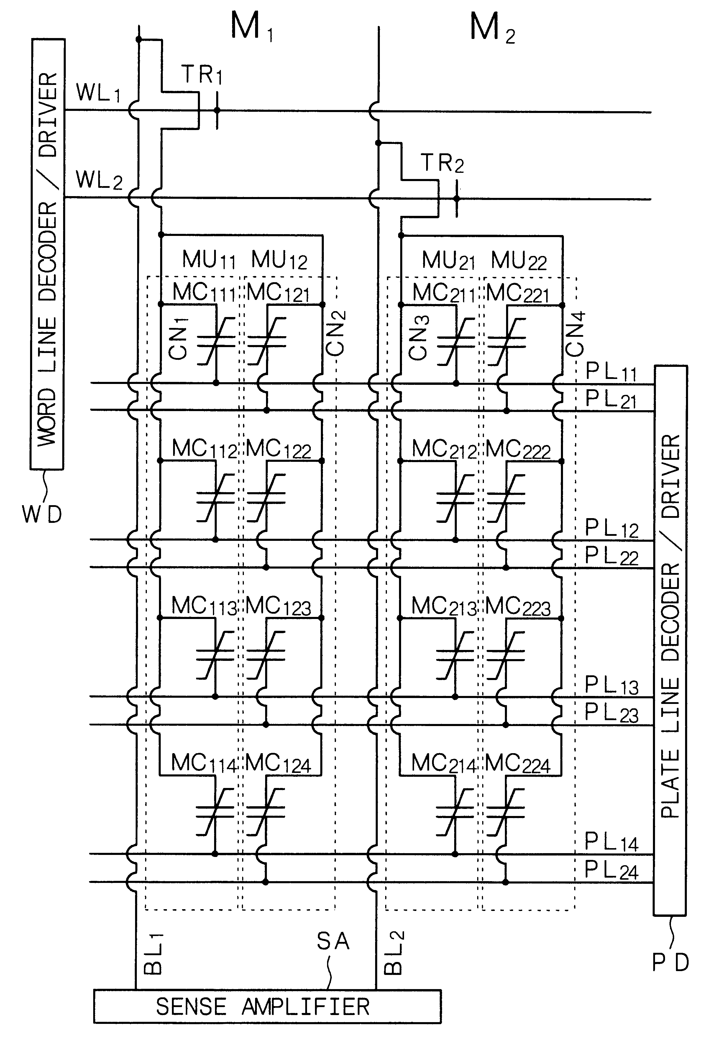
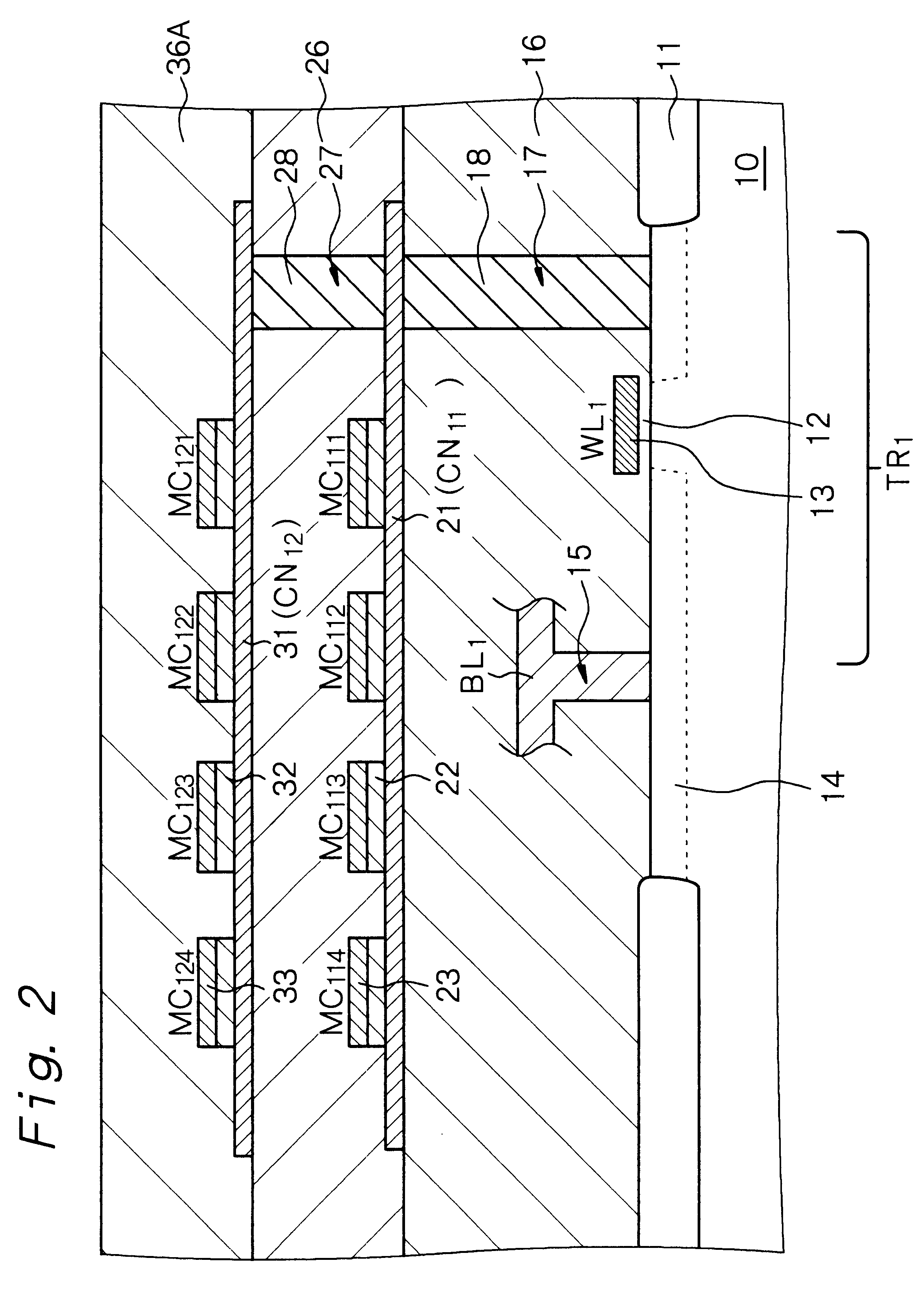
is concerned with the ferroelectric-type nonvolatile semiconductor memory (to be referred to as "nonvolatile memory" hereinafter) according to the first and sixth aspects of the present invention. FIG. 1 shows a circuit diagram of the nonvolatile memory in Example 1, and FIG. 2 shows a schematic partial cross-sectional view thereof. While FIG. 1 shows the two nonvolatile memories M.sub.1 and M.sub.2, these nonvolatile memories have the same circuits. The following explanation will discuss the nonvolatile memory M.sub.1.

The above nonvolatile memory M.sub.1 comprises a bit line BL.sub.1, a transistor for selection TR.sub.1 made of a MOS type FET, memory units in the number of N (provided that N.gtoreq.2, and N=2 in Example 1) or memory units MU.sub.11 and MU.sub.12, and plate lines. The memory unit MU.sub.11 comprises memory cells in the number of M (provided that M.gtoreq.2, and M=4 in Example 1) or memory cells MC.sub.11m (m=1, 2, 3, 4). The memory unit MU.sub.12 also comprises memo...

example 2

Example 2 is concerned with the nonvolatile memory according to the second aspect of the present invention. FIG. 5 shows a circuit diagram of the nonvolatile memory in Example 2, and FIG. 6 shows a schematic partial cross-sectional view thereof. While FIG. 5 shows two nonvolatile memories M.sub.1 and M.sub.2, these nonvolatile memories have the same circuits. The following explanation will discuss the nonvolatile memory M.sub.1.

The nonvolatile memory M.sub.1 comprises a bit line BL.sub.1, transistors for selection TR.sub.11 and TR.sub.12 made of MOS type FETs in the number of N (provided that N.gtoreq.2, and N=2 in Example 2), memory units MU.sub.11 and MU.sub.12 in the number of N (provided that N=2 in Example 2) and plate lines. The first memory unit MU.sub.11 comprises memory cells MC.sub.11m (m=1, 2, 3, 4) in the number of M (provided that M.gtoreq.2, and M=4 in Example 2). The second memory unit MU.sub.12 also comprises memory cells MC.sub.12m (m=1, 2, 3, 4) in the number of M ...

example 3

Example 3 is directed to a variant of the nonvolatile memory in Example 2. FIG. 9 shows a circuit diagram thereof, and FIG. 10 shows a schematic partial cross-sectional view thereof. In the nonvolatile memory in Example 3, the number N of memory units is four. That is, the nonvolatile memory comprises a bit line BL.sub.1, 4 transistors for selection TR.sub.1N, 4 memory units MU.sub.1N each of which comprises 8 memory cells MC.sub.1NM and 8 plate lines PL.sub.M.

Each memory cell MC.sub.1nm comprises a first electrode 21, 31, 41 or 51, a ferroelectric layer 22, 32, 42 or 52 and a second electrode 23, 33, 43 or 53. In each memory unit MU.sub.1n, the first electrodes of the memory cells MC.sub.1nm is in common. That is, they constitute a common node CN.sub.1n.

The common first electrode (common node CN.sub.1n) in the memory unit MU.sub.1n is connected to the bit line BL.sub.1 through the transistor for selection TR.sub.1n. In the memory unit MU.sub.1n, further, the second electrode of the...


PUM


Abstract

A ferroelectric-type nonvolatile semiconductor memory comprising (A) a bit line, (B) a transistor for selection, (C) memory units in the number of N, each memory unit including memory cells in the number of M wherein N>=2 and M>=2, and (D) plate lines in the number of MxN, in which the memory units in the number of N are stacked through an insulating interlayer, each memory cell includes a first electrode, a ferroelectric layer and a second electrode, the first electrodes are in common in each memory unit, and the common first electrode is connected to the bit line through the transistor for selection, and the second electrode of the m-th memory cell in the n-th memory unit is connected to the [(n-1)M+m]-th plate line wherein m=1, 2 . . . M and n=1, 2 . . . N.

Description

RELATED APPLICATION DATAThe present and foregoing application claim priority to Japanese Application Nos. P2000-156089 filed May 26, 2000, No. P2000-247143 filed Aug. 17, 2000, No. P2000-252080 filed Aug. 23, 2000, No. P2000-262755 filed Aug. 31, 2000 and No. P2000-317880 filed Oct. 18, 2000. All of the foregoing applications are incorporated herein by reference to the extent permitted by law.BACKGROUND OF THE INVENTION AND RELATED ART STATEMENTThe present invention relates to a ferroelectric-type nonvolatile semiconductor memory (so-called FERAM) and an operation method-thereof.In recent years, studies are actively made with regard to a ferroelectric-type nonvolatile semiconductor memory having a large capacity. A ferroelectric-type nonvolatile semiconductor memory (to be sometimes abbreviated as "nonvolatile memory" hereinafter) permits rapid access and is nonvolatile, and it consumes less electric power and has strength against an impact, so that it is expected to be used as a ma...

Claims


Application Information

Patent Timeline
Patent Type & Authority Patents(United States)
IPC IPC(8): H01L21/70H01L21/8246H01L27/115
CPCH01L27/11507H01L27/11502H10B53/30H10B53/00G11C11/22
Inventor NISHIHARA, TOSHIYUKIWATANABE, KOJI
Owner SONY CORP
Why Eureka
Try Eureka