Solid-state imaging device

a solid-state imaging and imaging device technology, applied in the direction of radio frequency controlled devices, instruments, lenses, etc., can solve the problems of heat resistance, spectral performance, and inability to completely condensate light reaching the microlens on a photodiode, etc., to achieve the effect of reducing the cost of operation, and improving the quality of operation

Inactive Publication Date: 2003-06-24
SOVEREIGN PEAK VENTURES LLC
View PDF18 Cites 76 Cited by
  • Summary
  • Abstract
  • Description
  • Claims
  • Application Information

AI Technical Summary

Problems solved by technology

However, because the microlens is weak in humidity, it is necessary to protect the microlens by any means when the lens is used under a severe condition such as high temperature and high humidity.
However, at the time of selecting a sealing resin for covering a microlens by considering heat resistance, transparency, spectral performance, and refractive-index change, it is unavoidable to select a resin almost the same as the material of the microlens and thereby, the refractive index of the sealing resin bec

Method used


Image

  • Solid-state imaging device
  • Solid-state imaging device
  • Solid-state imaging device

Examples


Embodiment Construction

Hereafter, the present invention will be more minutely described in accordance with embodiments. However, the present invention is not restricted to the following embodiments.

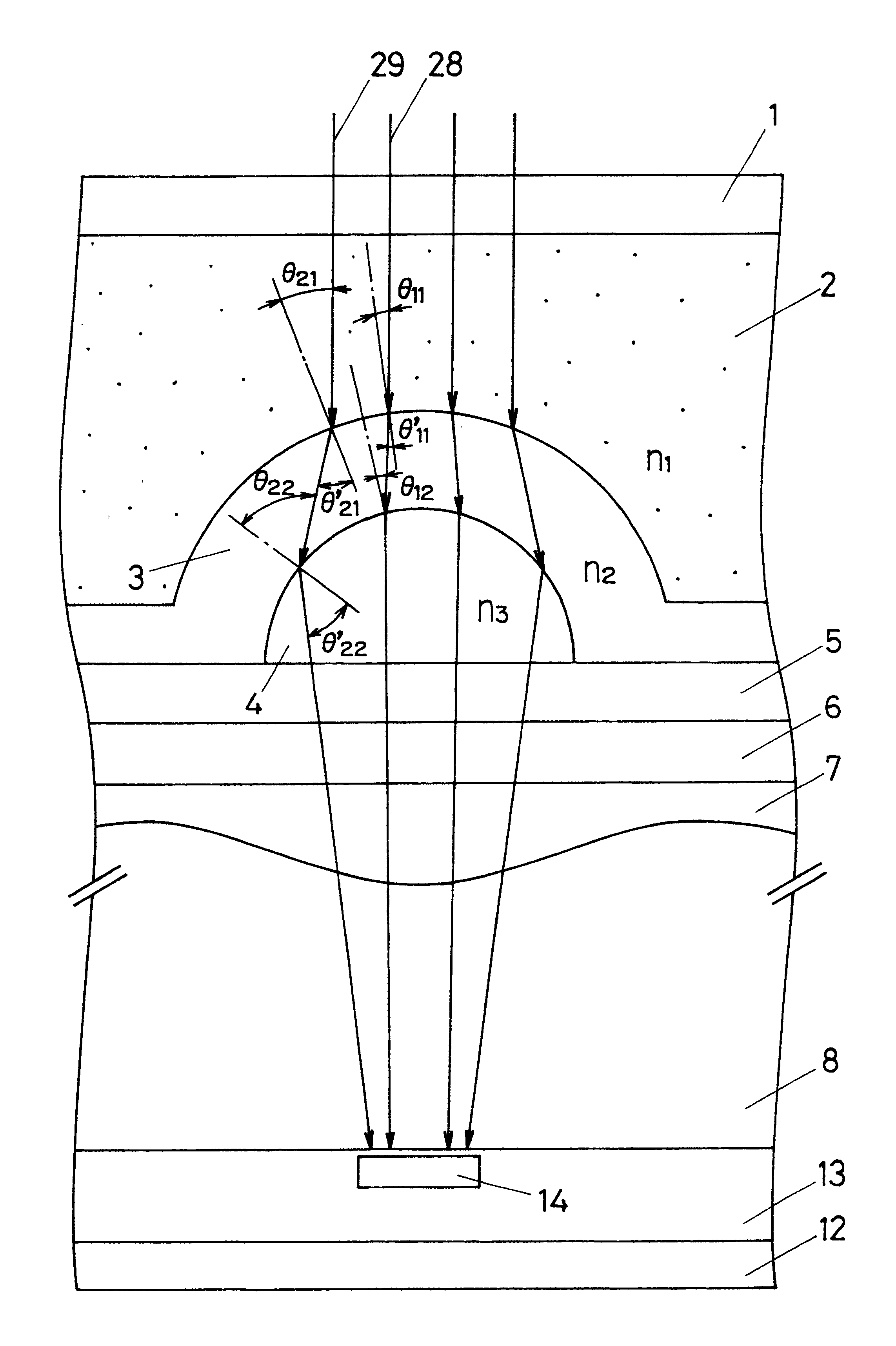
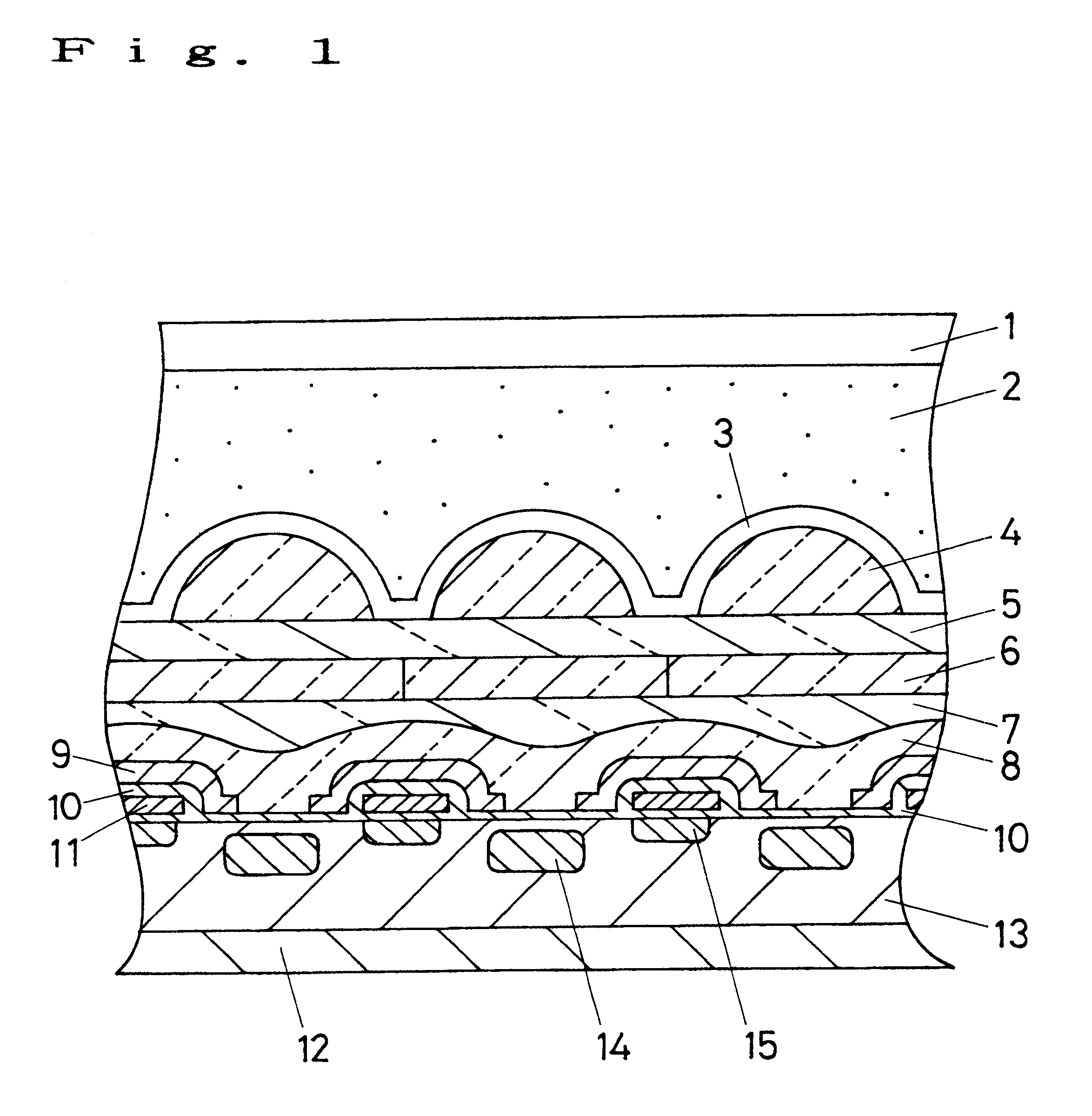
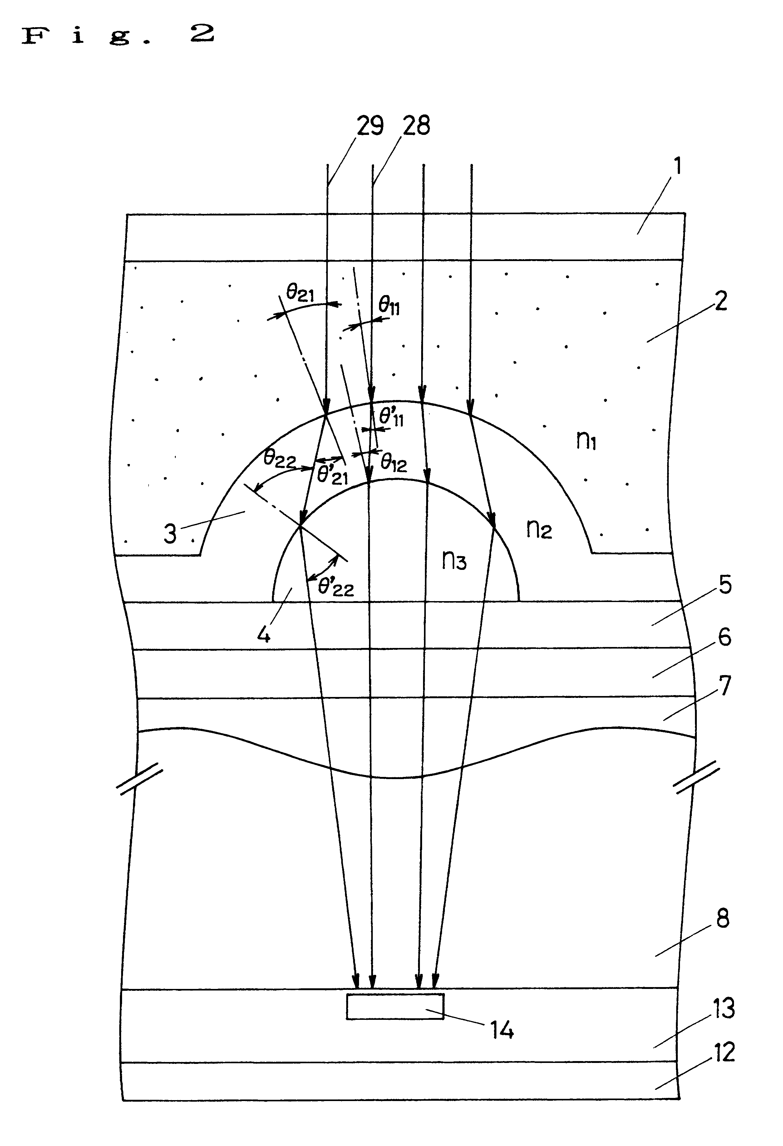
First, as shown in FIG. 1, the photodiode 14 serving as a light-receiving portion which is an n-type impurity area is formed in the p-type well layer 13 formed on the surface layer of the n-type semiconductor substrate 12 together with the vertical transfer register 15 and the like through the ion implantation method.

Then, a silicon-oxide film is formed through the thermal oxidation method, moreover a silicon-nitride film is formed on the silicon-oxide film through the chemical vapor deposition method (CVD method) to use the silicon-nitride film as the insulating film 10. Then, a polycrystal-silicon film is formed on the silicon-nitride film (insulating film 10) through the CVD method.

The upper portion of the photodiode 14 of the polycrystal-silicon film is removed through etching and further thermally oxidized...


PUM


Abstract

A conventional solid-state imaging device in which a sealing resin is applied onto a microlens has a low condensing efficiency. There are provided a photodiode 14 for receiving light, a microlens 4 made of a resin set on the photodiode 14 and having a refractive index of n3, a thin-film lens 3 formed on the microlens 4 and having a refractive index of n2, a sealing resin 2 formed on the thin-film lens 3 and having a refractive index of n1, and cover glass 1 formed on the sealing resin 2 to seal the sealing resin 2. The refractive index n2 of the thin-film lens 3 is set to a value smaller than n1 and n3. In this case, it is assumed that values of n1 and n3 are substantially equal to each other and the thin-film lens 3 is made of fluoride and/or oxide.

Description

1. Field of the InventionThe present invention relates to a solid-state imaging device having a microlens and sealing resin on the microlens.2. Description of the Prior ArtAs for a solid-state imaging device using a CCD (Charge Coupled Device), the area of a photodiode serving as a light-receiving portion has been decreased because of requests for decrease in size and improvement in resolution. To compensate the deterioration of a condensing efficiency due to decrease of the area of the light-receiving portion, the so-called microlens has been developed and used.The microlens is normally made of resin and set above a light-receiving portion formed for each pixel to directly refract light not incoming to the light-receiving portion, to condense the light in the light-receiving portion, and to improve the condensing efficiency and the sensitivity.However, because the microlens is weak in humidity, it is necessary to protect the microlens by any means when the lens is used under a seve...

Claims


Application Information

Patent Timeline
IPC IPC(8): G02B3/00H01L31/0232H01L27/146
CPCG02B3/0012H01L31/0232H01L27/1462H01L27/14627G02B3/005G02B3/0006H01L31/02327
Inventor UCHIDA, SHINJI
Owner SOVEREIGN PEAK VENTURES LLC
Why Eureka
Try Eureka