Photoconductive switching element, device using it, and apparatus, recording apparatus, and recording method in which the device is incorporated

a technology of photoconductive switching element and device, which is applied in the direction of static indicating device, photomechanical device, instrument, etc., can solve the problems of poor sensitivity, disadvantageous rectification function and disadvantage of organic photoconductive switching elemen

Inactive Publication Date: 2003-07-29
FUJIFILM BUSINESS INNOVATION CORP
View PDF15 Cites 46 Cited by
  • Summary
  • Abstract
  • Description
  • Claims
  • Application Information

AI Technical Summary

Problems solved by technology

However, the organic photoconductive switching element is disadvantageous as described hereunder.
In detail, the rectification function of the organic photoconductive switching element is a disadvantage.
Though some materials such as polycarbazole can: be involved in bipolar transfer, the sensitivity is poor and such a material has not been used practically.
The reason in that the applied voltage is increased and the baking of an image is caused concomitantly.
In detail, when a voltage is applied on OPC which has rectification function, the time during which an electric field is applied to a liquid crystal effectively is reduced because the positive and negative bipolar voltage application is difficult.
Because of the rectification function, the electric filled of one polarity cannot be applied and a DC bias is applied to the liquid crystal equivalently in the effect, ions in the liquid crystal are transferred to the place near the electrode because of the bias, the switching becomes difficult due to the electric field which ions generate, and the image baking occurs.
It is difficult to use not only the liquid crystal but a...

Method used


Image

  • Photoconductive switching element, device using it, and apparatus, recording apparatus, and recording method in which the device is incorporated
  • Photoconductive switching element, device using it, and apparatus, recording apparatus, and recording method in which the device is incorporated
  • Photoconductive switching element, device using it, and apparatus, recording apparatus, and recording method in which the device is incorporated

Examples


first embodiment

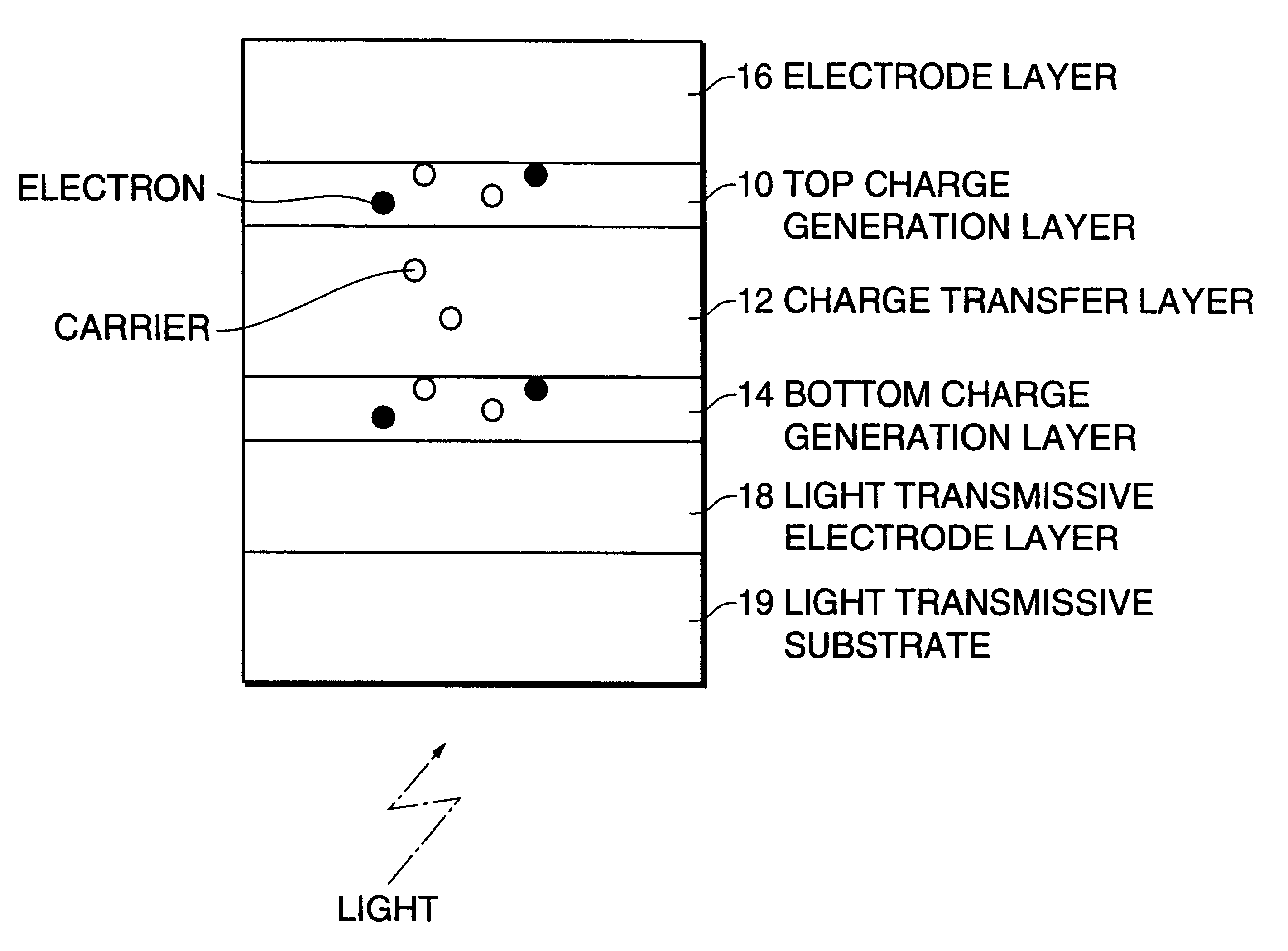
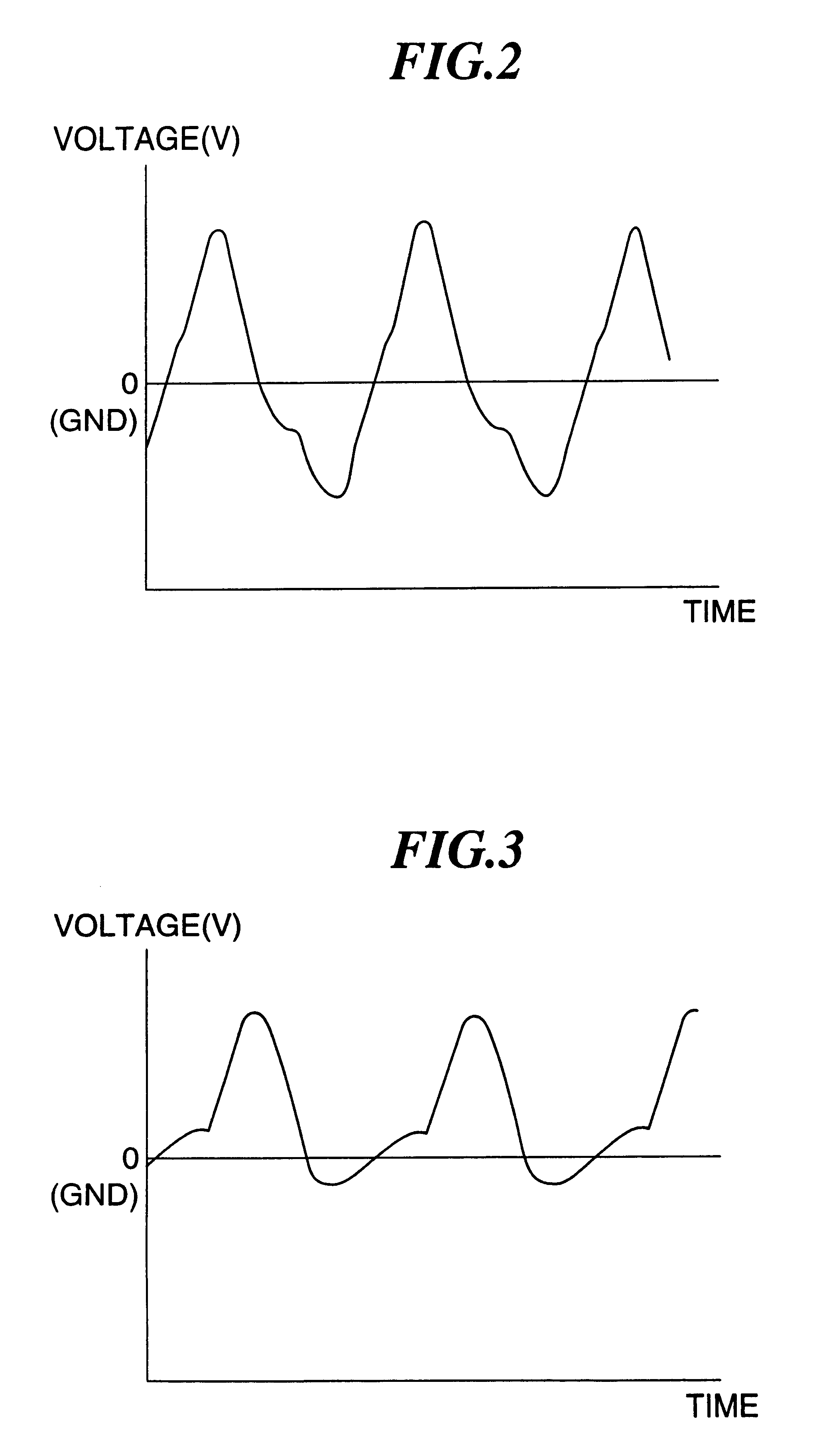
In this example, an organic photoconductive switching element was fabricated and electrodes were formed, and the waveform obtained when an AC voltage was applied on the photoconductive switching element under irradiation of light onto the photoconductive switching element was evaluated.

A benzimidazole perylene (referred to as "BZP" hereinafter) film having a thickness of 0.08 .mu.m was formed as the bottom charge generation layer by means of vacuum deposition on a glass substrate (product of DOW CORNING, 7059) having an ITO film formed thereon. Next, a solution containing 7.2% of 3,3'-dimethyl-N, N'-bis (4-ethylphenyl)-N, N'-bis (4-methylphenyl)-[1,1'-biphenyl]-4,4'-diamine (referred to as "biphenyldiamine base material" hereinafter), 10.8% of bis-phenol (Z) polycarbonate (referred to as "polycarbonate Z" hereinafter), and 82% of monochlorobenzene was diluted to 1 / 2 concentration of the original solution with monochlorobenzene, and the diluted solution was coated on the bottom charg...

second embodiment

A photoconductive switching element and an OPC cell were fabricated in the same manner as used in the first embodiment excepting that a dispersion containing chloro gallium phthalocyanine and binder was used as the material for the bottom charge generation layer and top charge generation layer and the top and bottom charge generation layers having a thickness of 0.25 .mu.m were formed by use of the dispersion and by means of spin coating as the film forming method.

third embodiment

A photoconductive switching element and an OPC cell were fabricated in the same manner as used in the first embodiment excepting that a dispersion containing azo base charge generation material and binder was used as the material for the bottom charge generation layer and top charge generation layer and the top and bottom charge generation layers having a thickness of 0.73 .mu.m were formed by use of the dispersion and by means of spin coating as the film forming method.


PUM


Abstract

The invention provides a photoconductive switching element used for light switching of a functional element driven by an AC electric field or AC current which are highly functional and inexpensive and provides a device in which such a photoconductive switching element and a functional element such as a liquid display element are combined and incorporated, and an apparatus, a recording apparatus, and a recording method which are provided with the above-mentioned device. The photoconductive switching element has at least a light transmissible electrode layer, a charge generation layer, a charge transfer layer, and a charge generation layer laminated in this order on a light transmissible substrate. The photoconductive switching element is combined with a functional element to form a device of the present invention, and the device is incorporated in an apparatus or a recording apparatus to fabricate an apparatus or a recording apparatus respectively of the present invention. In the recording method of the present invention, such a recording apparatus is used.

Description

1. Field of the InventionThis invention relates to a light switching element which uses an organic photoconductor, and a device, an apparatus, a recording apparatus, and a recording method which uses the light switching element.2. Description of the Related ArtRecently, an optically writable space modulation device which is a combination of a photoconductive switching element and a functional element such as a display element has been developed, and has been practically used for a projector as a light valve, and the possibility of application in the optical information process has been studied as described in "Liquid Crystal Space Modulator", Liquid Crystal, Vol. 2, No. 1, 1998, pp 3-18.In an optically writable space modulation device, the impedance of a photoconductive switching element is varied depending on the quantity of received light while a predetermined voltage is being applied on the element, the voltage applied on a display element is controlled to drive the display eleme...

Claims


Application Information

Patent Timeline
IPC IPC(8): H04N15/00G02F1/135G02F1/139
CPCG02F1/1354G02F1/1391
Inventor KOBAYASHI, HIDEOKAKINUMA, TAKEOKOSHIMIZU, MINORUHARADA, HARUOARISAWA, HIROSHI
Owner FUJIFILM BUSINESS INNOVATION CORP
Why Eureka
Try Eureka