
Reticle and direct lithography writing strategy

a writing strategy and lithography technology, applied in the field of reticle and direct lithography writing strategy, can solve the problems of increasing the enhancement factor of the mask, the difference in criticality is much less than might be expected, and the near future disappearance of any size error in the mask,

Inactive Publication Date: 2003-08-12
ASML NETHERLANDS BV
View PDF32 Cites 35 Cited by
  • Summary
  • Abstract
  • Description
  • Claims
  • Application Information

AI Technical Summary

Benefits of technology

This approach allows for the production of reticles with precise critical dimensions and small feature sizes, reducing variations and interference effects, thereby improving critical dimension uniformity and line resolution, and is suitable for various energy sources, enhancing the ability to produce masks with fine features and tight tolerances.

Problems solved by technology

However, the difference in criticality is much less than might be expected and will in the near future disappear.
It has been observed that nonlinearities in transfer of a pattern from a reticle to a wafer magnify any size errors in the mask.
At the same time, the mask error enhancement factor is likely to increase due to more aggressive lithographic process trade-offs, such as tuning the lithographic process to optimize the manufacture of contact holes, transistors or other critical features in order to use feature sizes closer to the theoretical resolution limit.
The requirements in pattern generators for patterning of reticles are so different than in steppers that chemically amplified resists are unsuitable for patterning reticles.
Work to modify conventional Novolac-DNQ resist to produce a resist suitable for DUV exposure of mask patterns reportedly has failed.
Uniformity and feature size requirements have become so demanding that wet etching no longer is suitable.
Wet etching is generally not useable when the size of features approach the thickness of the films the features are etched from.
It is difficult to compensate for this deviation by changing the data or the dose.
No non-amplified resist formulation is known which combines good contrast with high transparency.
The uniformity of resist erosion is difficult to control since, among other things, it depends on the pattern to be etched.
This erosion problem is exacerbated by the high optical absorption of non-chemically amplified resists used with DUV radiation.
Resist sidewall deviation from 90.degree. vertical inevitably limits the line resolution.
Using current chemistry it is not possible to make the resist thinner than 0.4-0.5 microns and still protect the chrome during the dry etching.
If the line at the top of the resist layer is narrowed, the wall angle less favorable or the resist thicker, the line would tend to vanish.
Obviously, each of the problems described gets worse as line widths get smaller, tolerances diminish, and the wavelength move into the deep ultraviolet.
The use of chemically amplified resists introduces other problems.
Use of chemically amplified resists on reticles is much more difficult than on wafers, due to the thickness and shape of reticles.
Reticles are much thicker and less thermally conductive than silicon wafers, making it more difficult to control the baking sequence accurately.
Furthermore, reticles are square, leading to corner effects that are not experienced with round wafers.
These post-exposure bake problems are not necessarily limited to chemically amplified resists, but are particularly had for chemically amplified resists due to the criticality of the baking step.
Non-chemically amplified resists are sometimes baked after exposure to even out standing wave interference effects, leading to the same problems.
Post-exposure baking also introduces a latent image diffusion problem, for both kinds of resist, but worse for the chemically amplified resists since the deactivation post bake often requires a substantially different temperature than that optimized for standing wave reduction.
An additional problem of chemically amplified resists is their instability and short working life.
This makes the current generation of chemically amplified resists unsuitable for use in a mask writer, which may take one to ten hours or more to write a mask and typically operates without an automated processing line.
The related problem is that the time from prebaked to post bake depends on the pattern written and is highly variable.
All single layer resists share properties that makes them less suitable in the foreseeable future.
As features get very small, wet developed resist structures assume an unfavorable aspect ratio.
In a mask pattern with 10 billion features it is highly likely that some of these high aspect ration features will be damaged by hydrodynamic forces and surface tension during wet processing.
The thin resist layer needs to be transparent to be exposed from top to bottom, but the transparency makes it subject to optical interference that lowers the effective performance of the resist and increases process variability.
The standing wave effect results from interference within the resist layer between light directed toward the reticle's surface and light reflected back.
With certain thicknesses of resist, there is destructive interference between the light entering and leaving the resist, allowing a maximum number of photons to stay in the resist layer, producing high sensitivity.
Variations in the resist bulk or thickness effect the sensitivity of the film and lead to non uniformity is in the pattern produced.
These problems are common to ordinary and chemically amplified resists.
Mask production faces additional issues.
For instance, production control is difficult due to low production volume.
Monitoring and feedback techniques used to improve the quality of semiconductor production are not readily applied to low volume production.

Method used


Image

  • Reticle and direct lithography writing strategy
  • Reticle and direct lithography writing strategy
  • Reticle and direct lithography writing strategy

Examples


Embodiment Construction

and embodiments practicing the invention is made with respect to the figures. It is presented for purposes of illustration and description. It is not intended to limit the invention to the precise forms disclosed. Many modifications and equivalent arrangements will be apparent to persons of ordinary skill in the art.

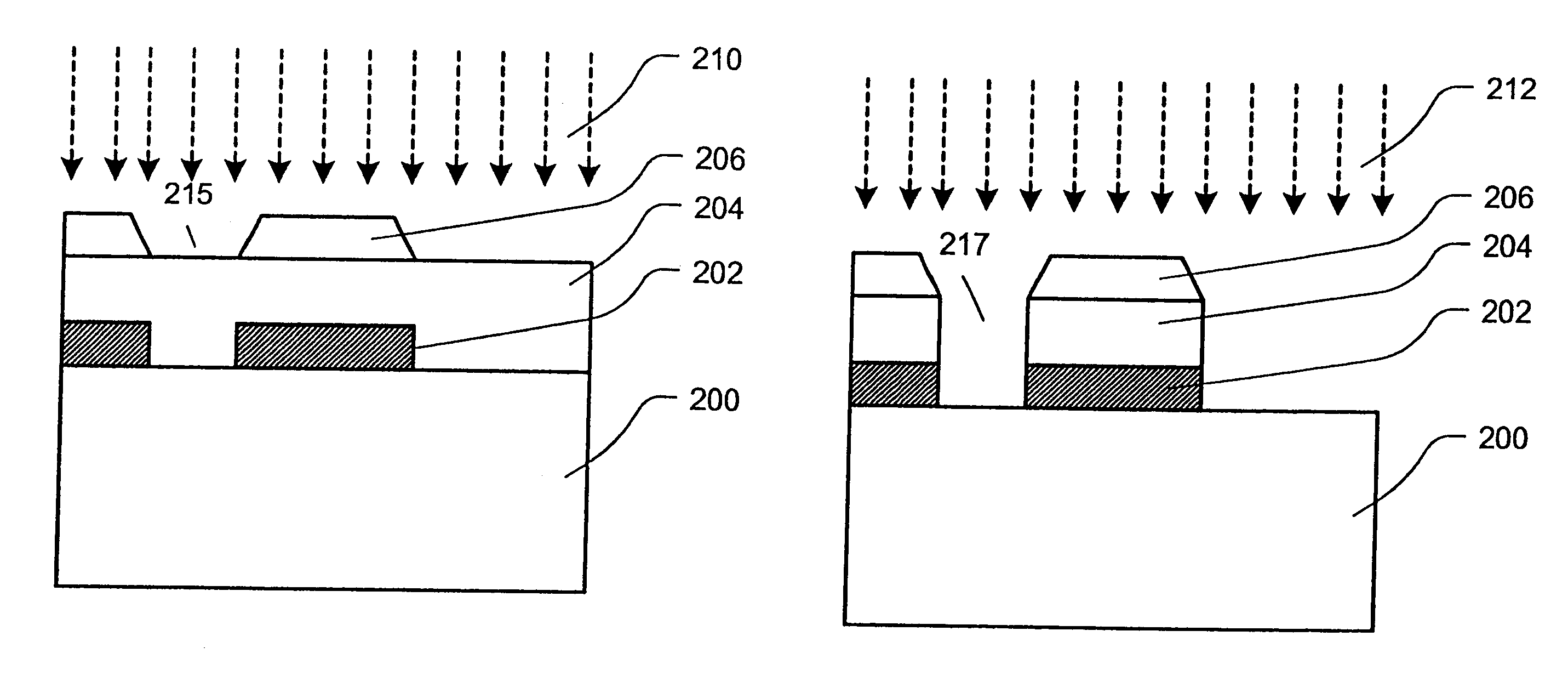
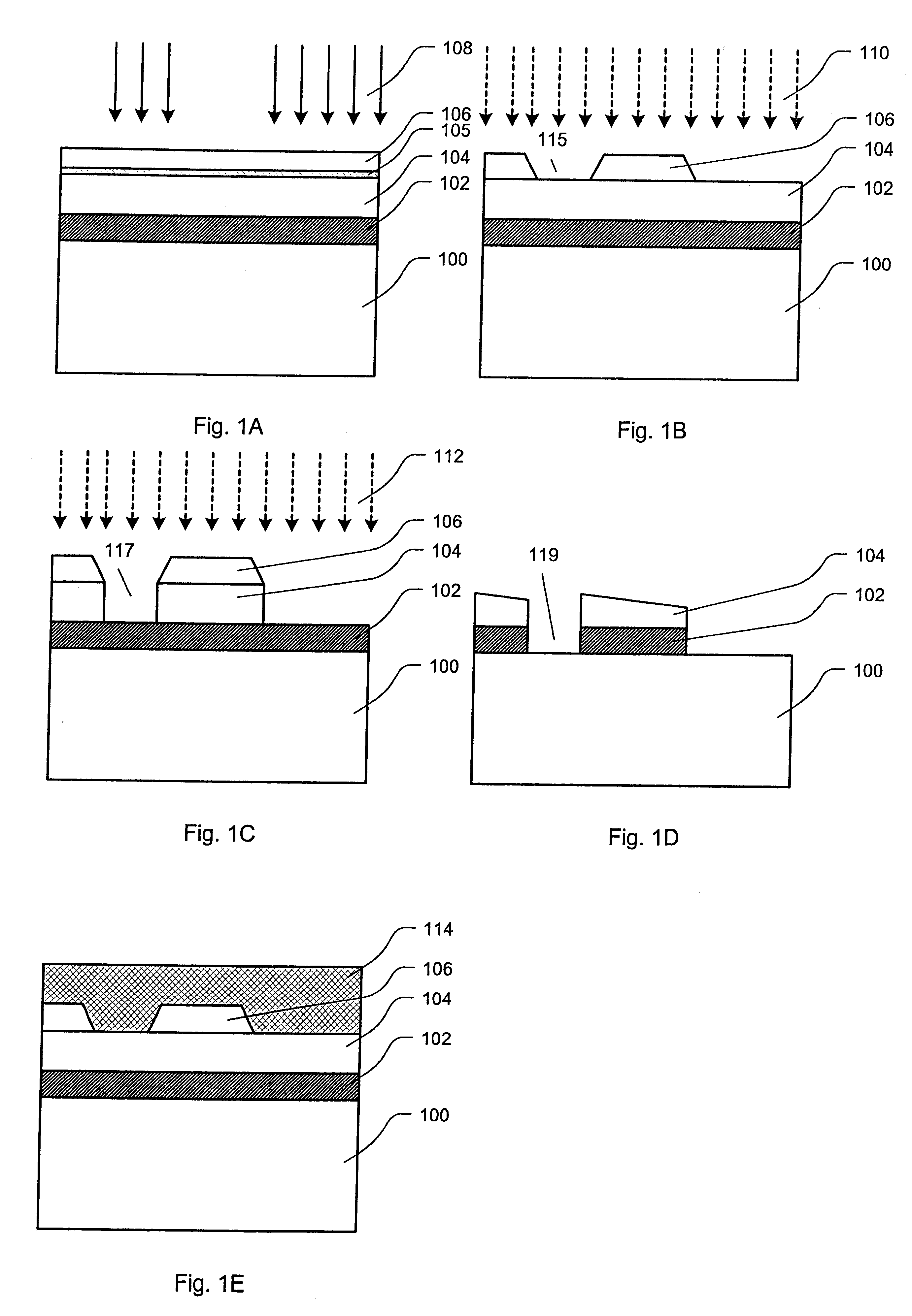
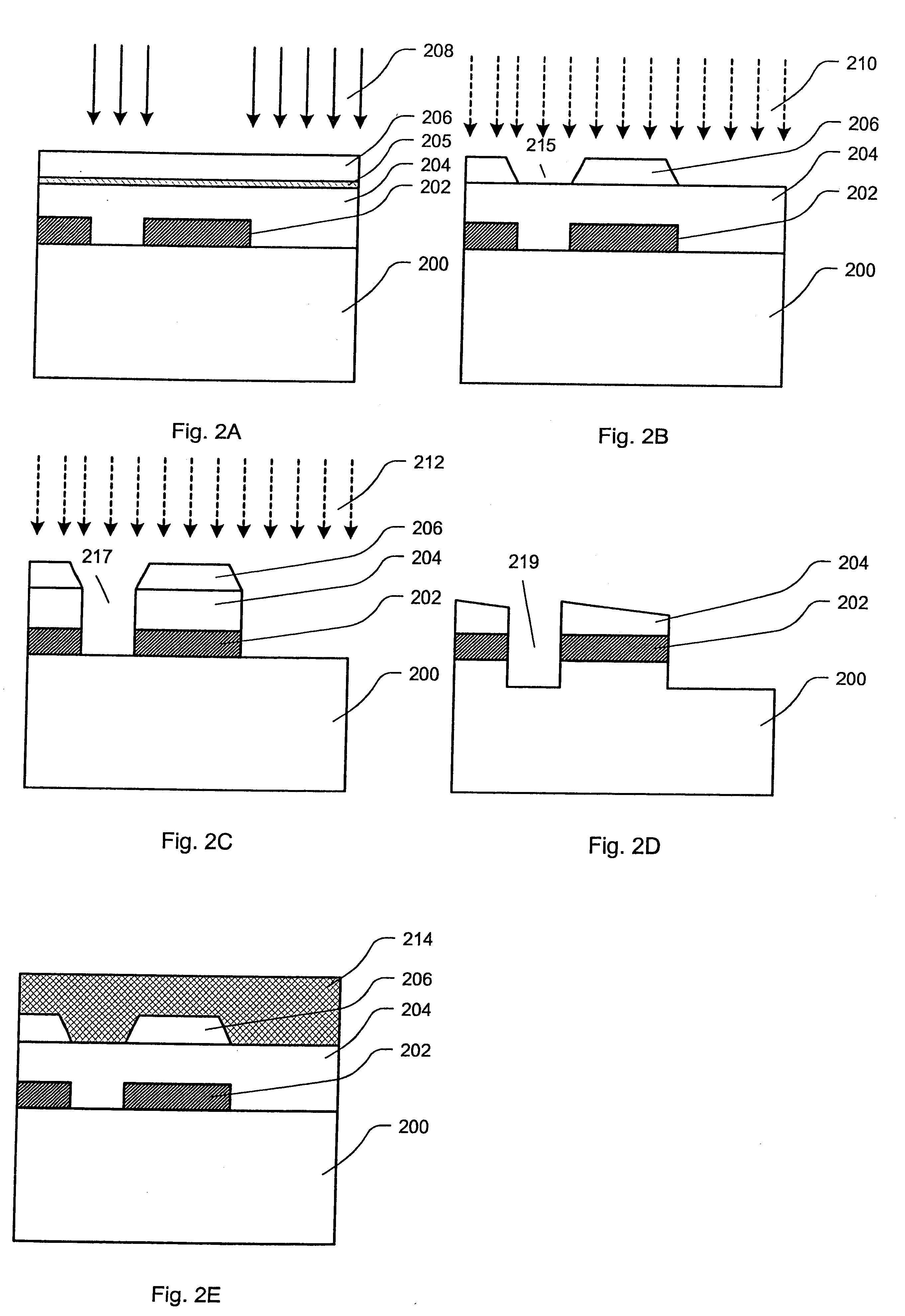
FIGS. 1A through 1E depict a coated reticle blank and process steps for a method of removing a non-transmissive layer from the surface of the reticle. In FIG. 1A, the coated reticle comprises a reticle blank 100, a masking or non-transmissive layer 102, a transfer layer 104, and a resist layer 106. Optionally, it may include a plasma resistive layer 105 between the transfer layer 104 and the resist layer 106. The reticle blank 100 often comprises a quartz substrate, a Zerodun.TM. ceramic substrate or an ULE.TM. glass substrate. One form factor currently used is 152 mm by 152 mm by 6.25 mm thick. In one style of mask, the blank is transmissive to an energy beam used durin...


PUM

PropertyMeasurementUnit
widthsaaaaaaaaaa
wavelength rangeaaaaaaaaaa
thicknessaaaaaaaaaa

Abstract

The present invention relates to preparation of patterned reticles to be used as masks in the production of semiconductor and other devices. Methods and devices are described utilizing resist and transfer layers over a masking layer on a reticle. The methods and devices produce small feature dimensions in masks and phase shift masks. The methods described for masks are in many cases applicable to the direct writing on other workpieces having similarly small features, such as semiconductor, cryogenic, magnetic and optical microdevices.

Description

The present invention relates to preparation of patterned reticles to be used as masks in the production of semiconductor and other devices. Methods and devices are described utilizing resist and transfer layers over a masking layer on a reticle.RELATED ARTSemiconductor devices include multiple layers of structures. The structures are formed in numerous steps, including steps of applying resist, then exposing, developing and selectively removing the resist to form a pattern of exposed areas. The exposed areas may be etched to remove material or sputtered to add material. A critical part of forming the pattern in the resist is exposing it. Resist is exposed to an energy beam that changes its chemical properties. One cost-effective way of exposing the resist is with a stepper. A stepper uses a reticle, which typically includes a carefully prepared, transmissive quartz substrate overlaid by a non-transmissive or masking layer that is patterned with areas to be exposed and areas to be l...

Claims


Application Information

Patent Timeline
Patent Type & Authority Patents(United States)
IPC IPC(8): G03F7/20G03F1/14G03F7/09G03F1/00G03F1/26G03F1/34G03F1/68G03F1/78H01L21/027H01L21/3065
CPCG03F1/14G03F1/26G03F1/34G03F1/68G03F1/78G03F7/094G03F7/2053G03F7/2063Y10S430/143G03F1/36G03F1/76G03F7/162G03F7/168
Inventor SANDSTROM, TORBJORN
Owner ASML NETHERLANDS BV
Learn More