Apparatus, manufacturing method and driving method of plasma display panel

a technology of plasma display panel and manufacturing method, which is applied in the direction of instruments, discharge tube luminescnet screens, and electrodes, etc., can solve the problems of short operation life, increased damage to the protection layer caused by ion impact, and low luminan

Inactive Publication Date: 2003-09-02
PIONEER CORP
View PDF18 Cites 19 Cited by
  • Summary
  • Abstract
  • Description
  • Claims
  • Application Information

AI Technical Summary

Problems solved by technology

This results in a problem of a short operation life, due to degradation of the protection layer.
In the case of the planar discharge, therefore, damage of the protection layer caused by the ion impact becomes more severe.
Furthermore, there is also a problem of a low luminance and a low conversion efficiency from the electric power to the luminance, because the discharge region is narrow.
Furthermore, there is also a problem of complicated driving sequence and a complicated drive circuit, because the electrode pair causing write discharge 21 and sustaining discharge 22 lies at the same place.
This variation of the peak values destroys the uniformity in luminance in the displayed pictures.
The luck of uniformity in the pictures becomes serious, as the display area becomes larger, particularly in case of the AC discharge--PDP, wherein pulse discharge current is high.
In this case, however, the voltage for driving the PDP becomes very high.
Furthermore, there is a problem of complicated driving sequence and a drive circuit caused by the fact that an electrode pair generates the write discharge 21 and the sustaining discharge 22.
Furthermore, there is a problem that the luminance varies, depending upon the location on the display panel.
However, there is a disadvantage that the capacitance between data electrode 2, scan electrode 4 and common electrode 11 become large and hence the driving load increases.
This poses a serious problem especially in large area display panels.
Furthermore, since each discharge is of the planar discharge, the problem of the shortened life caused by degradation of a protection layer not easily solved.
A first problem is that the write voltage (a difference in peak value between the write pulse 18 and the signal pulse 19, in other words, the sum of respective absolute values) is high.
In the conventional technique, an inexpensive low withstanding voltage circuit cannot be used as a drive circuit for applying a voltage pulse to data electrode 2 and scan electrode 4, but an expensive high withstanding voltage circuit must be used.
Finally, this results in an increase of the manufacturing cost.
If the height of partition 6 is lowered, however, the discharge space becomes narrow, resulting in an evil influence of a raised sustaining voltage.
Consequently, it also causes a decrease in luminance and efficiency due to a decrease in the quantity of ultraviolet light.
A second problem is that it is dif...

Method used


Image

  • Apparatus, manufacturing method and driving method of plasma display panel
  • Apparatus, manufacturing method and driving method of plasma display panel
  • Apparatus, manufacturing method and driving method of plasma display panel

Examples


embodiment 1

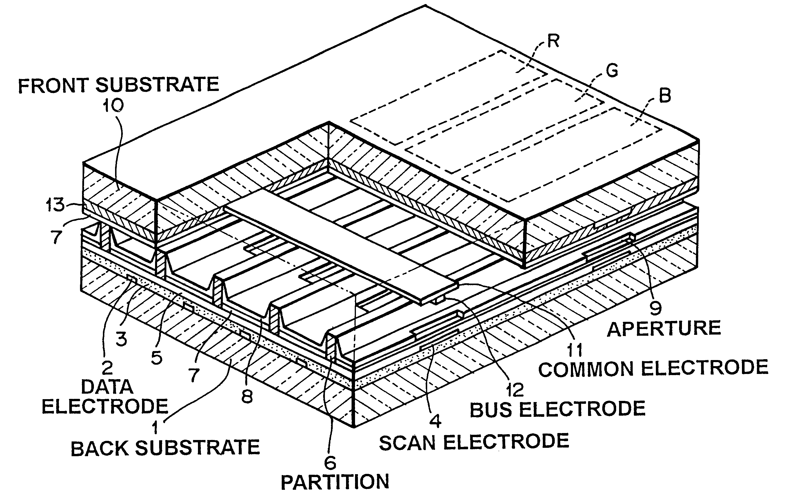
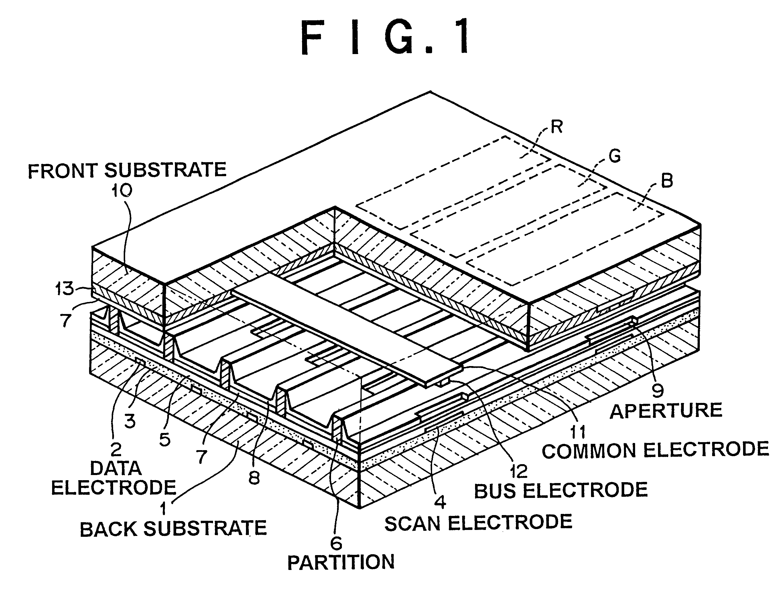
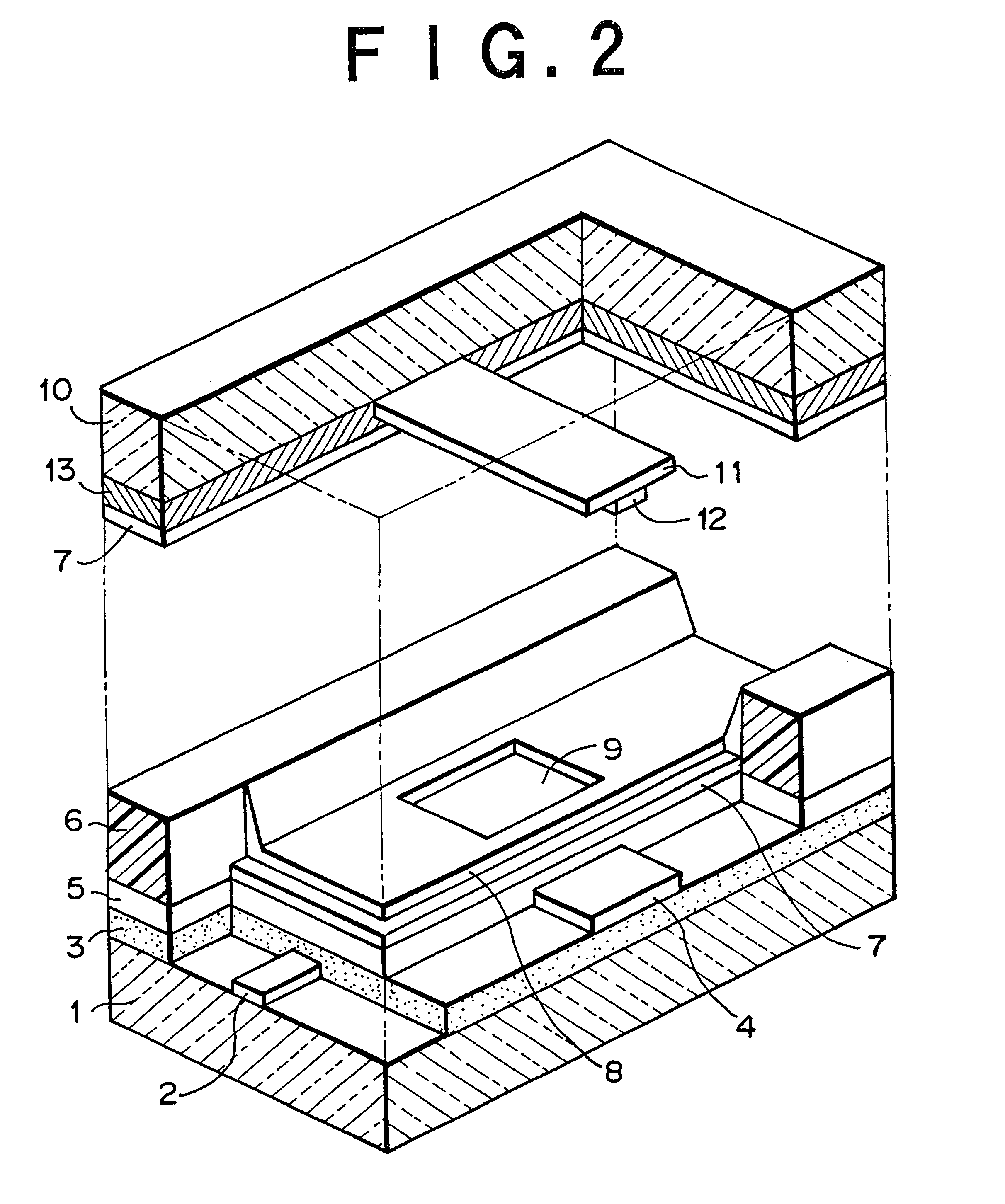
FIG. 1 is an exploded oblique view of a plasma display panel (PDP) according to the present invention. Furthermore, FIG. 2 is an exploded oblique view showing a unit cell structure of a PDP according to the present invention. By referring to FIGS. 1 and 2, the structure of the present invention will be described. On a back glass substrate 1, data electrodes 2 made of metal or the like are formed in the substrate column direction. Over the data electrodes 2, a dielectric layer 3 made of a metallic oxide or the like is formed. On the dielectric layer 3, scan electrodes 4 made of metal or the like are formed in a substrate row direction. Over the scan electrodes 4, a dielectric layer 5 made of a metallic oxide or the like is formed. On the dielectric layer 5, stripe-shaped partitions 6 made of a metallic oxide or the like are formed in the substrate column direction. On the dielectric layer 5 including side faces of the partitions 6, a protection layer 7 and a fluorescent material laye...

embodiment 2

FIG. 9 is an oblique view of another PDP according to the present invention. Furthermore, FIG. 10 is an exploded oblique view showing its unit cell structure. Unlike the embodiment 1, the embodiment 2 is not formed of two pieces, i.e., the front glass substrate 10 and the back glass substrate 1, but formed of three pieces including a center sheet 17 interposed between the front glass substrate 10 and the back glass substrate 1. By referring to FIGS. 9 and 10, a different structure of the present invention will be described. On the back glass substrate 1, data electrodes 2 made of metal or the like are formed in the substrate column direction. Over the data electrodes 2, a dielectric layer 3 made of a metallic oxide or the like is formed. On the dielectric layer 3, scan electrodes 4 made of metal or the like are formed in a substrate row direction. Over the scan electrodes 4, a dielectric layer 5 made of a metallic oxide or the like and a protection layer 7 are formed.

On the other ha...

embodiment 3

FIG. 12 is an oblique view of a different PDP according to the present invention. FIG. 13 is an oblique exploded view showing a unit cell structure. Unlike the embodiment 1 and the embodiment 2, in the embodiment 3, a common electrode 11 formed on the front glass substrate 10 side and a scan electrode 4 formed on the back glass substrate 1 side are not located in such positions that they are just opposed to each other. The common electrode 11 is formed with a shift in the cell longitudinal direction from the scan electrode 4. As for the structure of the present invention, the case where the PDP is manufactured by using the manufacturing method described with reference to the embodiment 1 is exemplified.

In the structure of the present invention, a sustaining discharge 22 is generated obliquely between the scan electrode 4 and the common electrode 11. Therefore, the sustaining discharge 22 looks as if it extends in the cell longitudinal direction. Even if the height of the partitions ...


PUM


Abstract

To provide a plasma display panel which improves the write characteristics, luminous luminance, and luminous efficiency and which has a longer life. On a back glass substrate, data electrodes are formed in the substrate column direction. Over the data electrodes, a dielectric layer is formed. On the dielectric layer, scan electrodes are formed in a substrate row direction. Over the scan electrodes, a dielectric layer is formed. On the dielectric layer, partitions are formed in the substrate column direction. On the dielectric layer including the partitions, a protection layer and a fluorescent material layer are formed. On the other hand, on a front glass substrate, common electrodes and bus electrodes electrically connected to the common electrodes are formed in the substrate row direction so as to be opposed to the scan electrodes. Over the common electrodes and the bus electrodes, a dielectric layer and a protection layer are formed.

Description

1. Technical Field of the InventionThe present invention relates to a plasma display panel (PDP), and in particular to a panel structure, its manufacturing method, its drive method, and its drive device which makes possible low voltage drive and fast writing, and which can achieve high luminance, a high efficiency, and a longer life.2. Description of the Prior ArtIn PDP, electrons accelerated by an electric field collide with gas atoms or molecules and ultraviolet light generated by the collision is converted to visible light by fluorescent materials to display color images. PDP is one of the flat panel display apparatuses with large area and large capacity. Conventional PDP is explained, referring to FIGS. 15 to 18. In these figures, the portions relating to various electrodes are mainly illustrated.In a structure shown in FIG. 15, data electrode 2 is formed in a column direction on back glass substrate 1. On data electrode 2, dielectric layer 3 is formed. On the dielectric layer 3...

Claims


Application Information

Patent Timeline
IPC IPC(8): G09G3/28G09G3/288G09G3/291G09G3/294G09G3/297H01J11/12H01J11/14H01J11/22H01J11/24H01J11/26H01J11/28H01J11/32H01J11/34H01J11/36H01J11/38H01J11/42H01J11/46
CPCG09G3/294H01J11/20H01J11/22G09G3/296
Inventor HIRANO, NAOTONUNOMURA, KEIJI
Owner PIONEER CORP
Why Eureka
Try Eureka