Integrated process for depositing layer of high-K dielectric with in-situ control of K value and thickness of high-K dielectric layer

a technology of high-k dielectric and in-situ control, applied in the direction of optical radiation measurement, semiconductor/solid-state device testing/measurement, instruments, etc., can solve the problems of new methods of fabrication or new arrangements, charge carriers to tunnel across gate oxide films, and transistor "leaky"

Inactive Publication Date: 2003-11-04
GLOBALFOUNDRIES US INC
View PDF11 Cites 95 Cited by
  • Summary
  • Abstract
  • Description
  • Claims
  • Application Information

AI Technical Summary

Benefits of technology

Thus, the present invention provides an apparatus and a control process which provides for precise, in-situ control and determination of the quality, thickness and K value of a film of a dielectric material, in particular of a high-K dielectric material, and which overcomes the problem of expensive and time-consuming physical measurement and electrical testing to determine the quality, thickness and K value of such films after completion of the deposition steps.

Problems solved by technology

As the devices and features shrink, and as the drive for higher performing devices escalates, new problems are discovered that require new methods of fabrication or new arrangements or both.
Decreasing the thickness of the gate oxide film between the gate electrode and the source / drain extension regions, together with the relatively high electric field across the gate oxide film, can undesirably cause charge carriers to tunnel across the gate oxide film.
This renders the transistor "leaky", degrading its performance.
One problem which has been encountered in fabricating semiconductor devices including high-K dielectric materials is dimensional control, particularly being able to obtain a desired thickness and a desired K value of high-K dielectric materials.

Method used


Image

  • Integrated process for depositing layer of high-K dielectric with in-situ control of K value and thickness of high-K dielectric layer
  • Integrated process for depositing layer of high-K dielectric with in-situ control of K value and thickness of high-K dielectric layer
  • Integrated process for depositing layer of high-K dielectric with in-situ control of K value and thickness of high-K dielectric layer

Examples


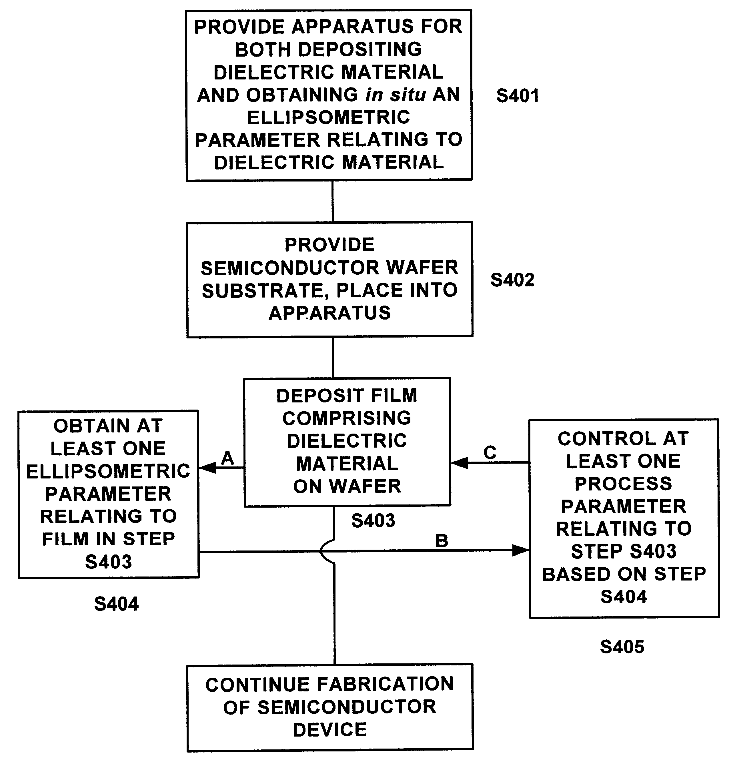
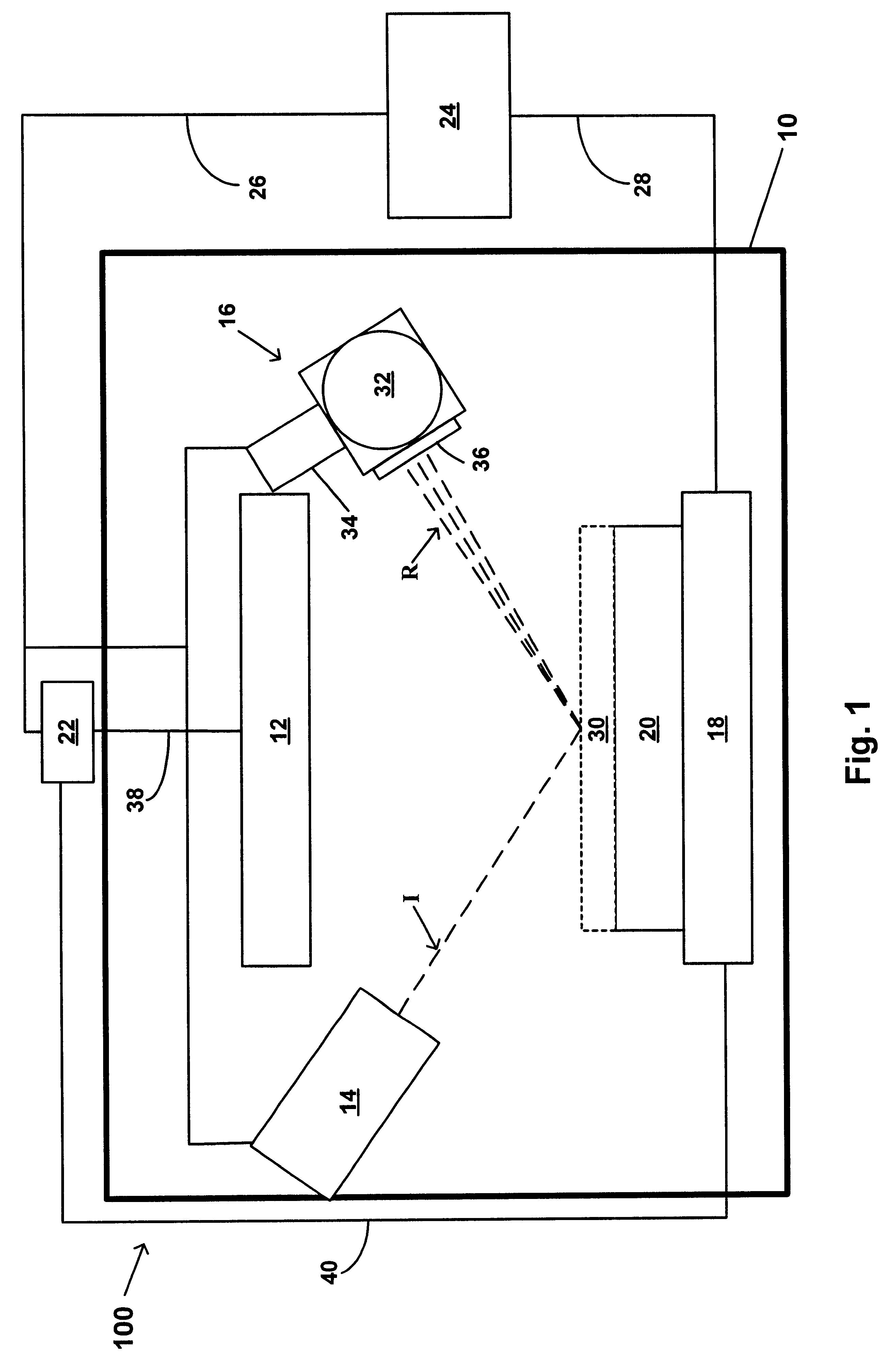
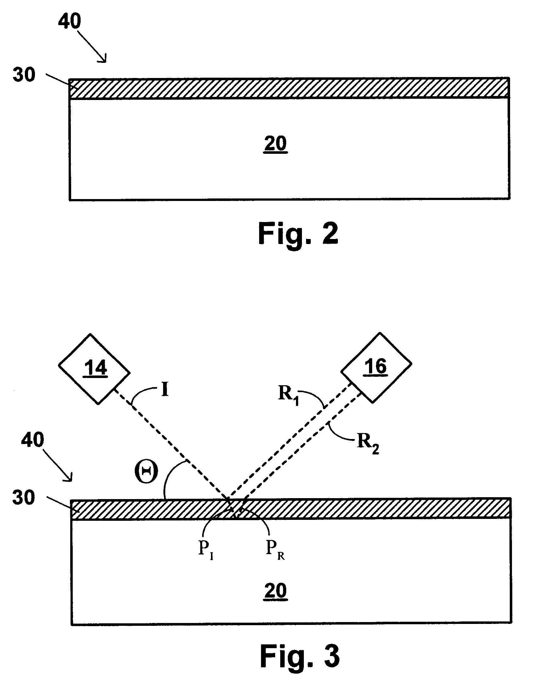
Embodiment Construction

As used herein, the term "standard-K dielectric material" refers to a dielectric material having a K up to about 10. Such standard-K dielectric materials include, for example, silicon dioxide, which has a K of about 4, silicon oxynitride, which has a K of about 4-8 depending on the relative content of oxygen and nitrogen, and silicon nitride, which has a K of about 6-9, and aluminum oxide, which has a K of about 10.

As used herein, the term "high-K dielectric material" refers to a dielectric material having a K greater than about 10. Such high-K dielectric materials include, for example, HfO.sub.2, ZrO.sub.2 and others known in the art, some of which are specifically identified more fully below. In general, the term "high-K dielectric material" encompasses binary, ternary and higher oxides and any ferroelectric material having a K of about 10 or more. High-K dielectric materials may also include, for example, composite materials such as hafnium silicate, which has a K of about 14, an...


PUM

PropertyMeasurementUnit
thicknessaaaaaaaaaa
thicknessaaaaaaaaaa
optical wavelengthsaaaaaaaaaa

Abstract

An apparatus and a method of depositing a dielectric material film, including steps of initiating a process of depositing a dielectric material film under at least one controllable initial condition in an apparatus comprising a dielectric material deposition chamber and a spectroscopic ellipsometer; and measuring, by the spectroscopic ellipsometer, at least one ellipsometric parameter of the dielectric material film during the process of depositing the film.

Description

The invention relates generally to the fabrication of semiconductor devices and, more particularly, to the fabrication of a dielectric material film for use in semiconductor devices.Fabrication of a semiconductor device and an integrated circuit thereof begins with a semiconductor substrate and employs film formation, ion implantation, photolithography, etching and deposition techniques to form various structural features in or on a semiconductor substrate to attain individual circuit components which are then interconnected to ultimately form an integrated semiconductor device. Escalating requirements for high densification and performance associated with ultra large-scale integration (ULSI) semiconductor devices requires smaller design features, increased transistor and circuit speeds, high reliability and increased manufacturing throughput for competitiveness. As the devices and features shrink, and as the drive for higher performing devices escalates, new problems are discovered...

Claims


Application Information

Patent Timeline
Patent Type & Authority Patents(United States)
IPC IPC(8): C23C16/52G01N21/21H01L21/00H01L21/02H01L21/316H01L21/314
CPCC23C16/52G01N21/211H01L21/67253H01L21/31691H01L21/31604H01L21/02183H01L21/02192H01L21/02142H01L21/02175H01L21/02145H01L21/02186H01L21/02211H01L21/02189H01L21/02205H01L21/02181H01L21/02271H01L21/02194H01L21/02197H01L21/02148
Inventor HALLIYAL, ARVINDARSANIA, FARZAD
Owner GLOBALFOUNDRIES US INC
Why Eureka
Try Eureka