Distributed feedback semiconductor laser device and multi-wavelength laser array

a semiconductor laser and laser array technology, applied in semiconductor laser arrangements, semiconductor lasers, optical resonator shape and construction, etc., can solve the problems of unsatisfactory economical standard, extreme difficulty, and the requirement of strict pitch control of diffraction gratings

Inactive Publication Date: 2003-11-04
FURUKAWA ELECTRIC CO LTD
View PDF8 Cites 8 Cited by
  • Summary
  • Abstract
  • Description
  • Claims
  • Application Information

AI Technical Summary

Benefits of technology

In accordance with the first invention, the layer having the function of controlling the equivalent refractive index can generate a plurality of the lasing wavelengths different among one another and easily controllable.
In accordance with the second invention, the distributed feedback semiconductor laser device of claim 1 disposed in the array overlying the common substrate can generate the lasing wavelengths different among one another to provide the multi-wavelength laser array which is easily fabricated and economical.

Problems solved by technology

However, in the first process, it is extremely difficult that the requirement of the strict pitch control of the diffraction grating is satisfied during the fabrication of the diffraction grating having a frequency spacing with 100 GHz (about 0.8 nm with 1.5 .mu.m wavelength range) level required for the high density WDM telecommunication system.
In order to conduct the strict pitch control, the expensive electron beam alignor is required, thereby dissatisfying the economical standard because the equipment cost is increased and the productivity is decreased.
Further, in the second process, the strict control of the thickness or the composition of the active layer by using the selective area growth method is difficult in reality, and the productivity thereof is low.

Method used


Image

  • Distributed feedback semiconductor laser device and multi-wavelength laser array
  • Distributed feedback semiconductor laser device and multi-wavelength laser array
  • Distributed feedback semiconductor laser device and multi-wavelength laser array

Examples


embodiment 2

of Multi-Wavelength Laser Array

A multi-wavelength laser array of the present embodiment has substantially same configuration and effect as those of the multi-wavelength laser array of Embodiment 1 except that a p-AlInAs oxidizable layer 24 acting as the non-Al oxide layer is used in place of the p-InP cladding layer 28a of Embodiment 1.

Embodiment 1 of Fabrication of Multi-Wavelength Laser Array

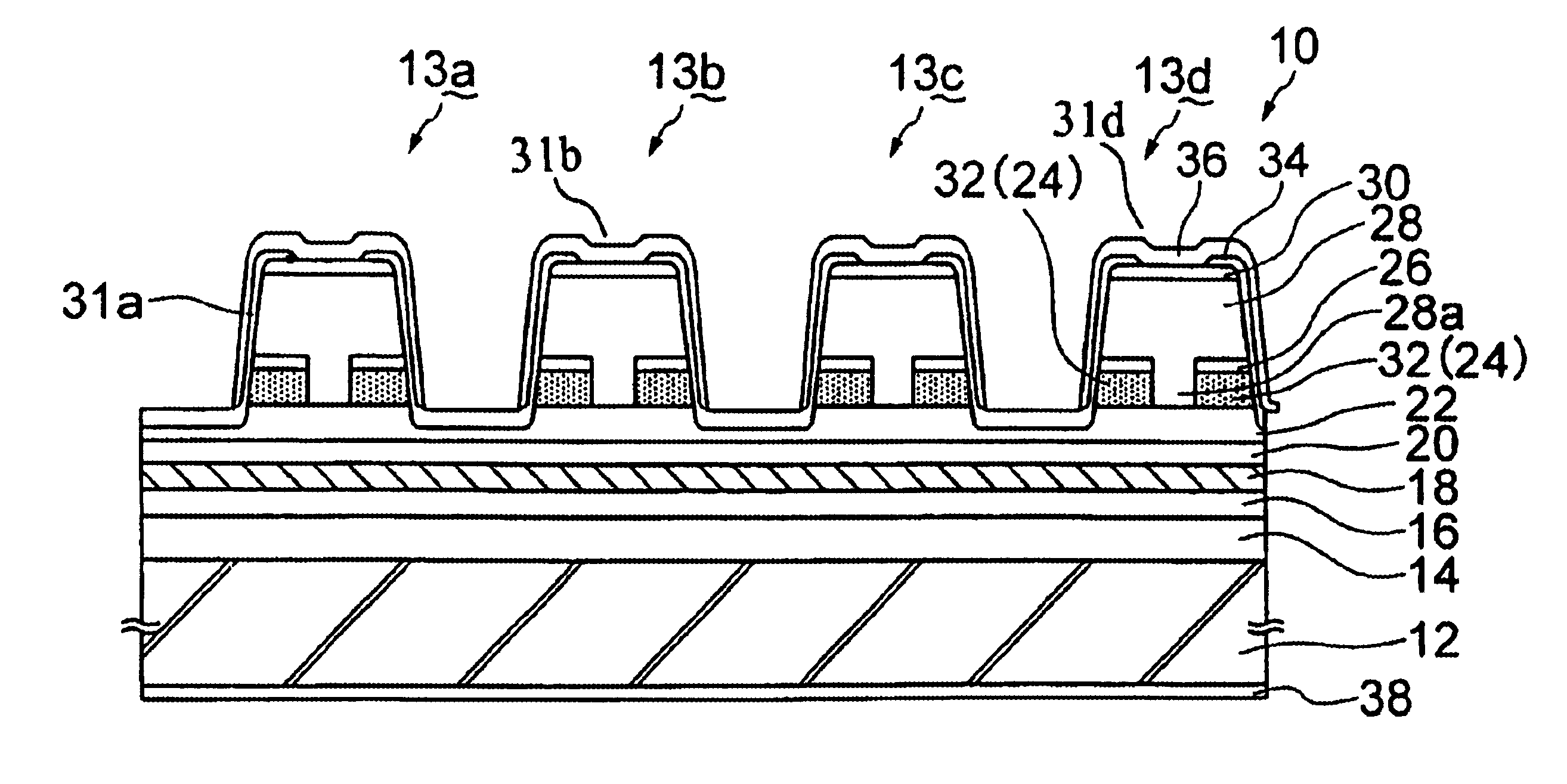
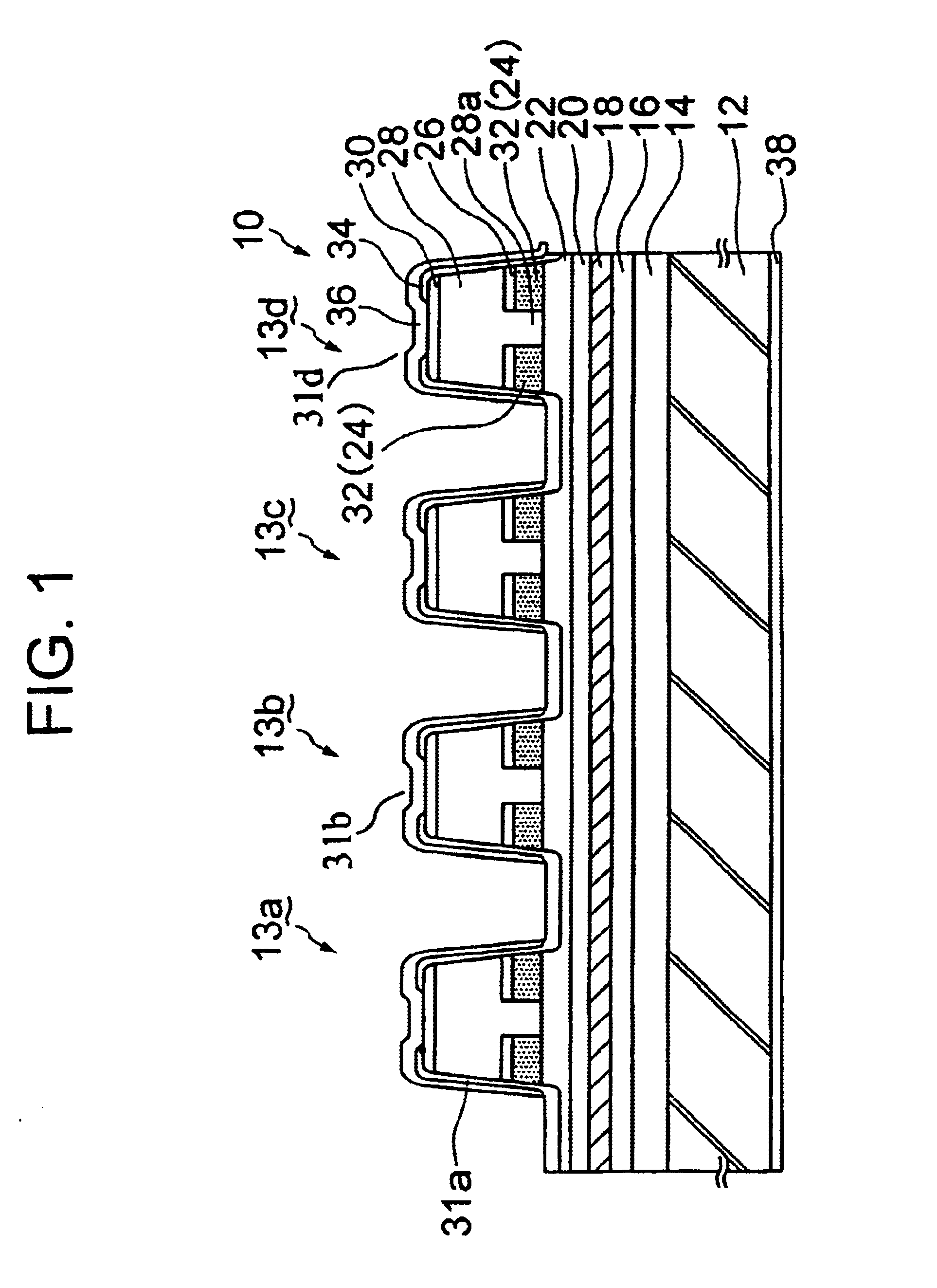
At first, as shown in FIG. 3A, an n-InP buffer layer 14, a non-doped GaInAsP layer 16 having a band gap wavelength of 1.1 .mu.m are grown on n-InP substrate in a first growth step. After forming uniform grating with a pitch of approximately 240 nm, a non-doped distortion quantum well active layer 18, a non-doped GaInAsP layer 20 having a band gap wavelength of 1.1 .mu.m, a p-InP cladding layer 22 having a thickness of 100 nm, a p-AlInAs oxidizable layer 24 having a thickness of 100 nm, and a p-GaInAsP layer 26 having a thickness of 30 nm are epitaxially grown and sequentially stacked on the In...

embodiment 1

of Fabrication of Multi-Wavelength Laser Array

A multi-layered structure shown in FIG. 3A is formed by the same procedures as those of the fabrication method of Embodiment 1 except that the p-AlInAs oxidizable layers 24 having the different thicknesses are formed on each of the semiconductor laser devices 13a to 13d by using the selective area growth method.

Without etching the p-AlInAs oxidizable layers 24 to form the channels 27, the p-InP cladding layer 28 and the p-GaInAs contact layer 30 are consecutively grown on the p-AlInAs oxidizable layer 24 in a second growth step by using the MOCVD method similarly shown in FIG. 3C.

Then, striped mesas having a width of 5 .mu.m are formed on each of the semiconductor laser devices 13a to 13d by etching the top portions of the contact layer 30, the p-InP cladding layer 28, the p-GaInAsP layer 26, the p-AlInAs oxidizable layer 24 and the p-InP cladding layer 22.

Then, the Al in the p-AlInAs oxidizable layer 24 is selectively oxidized under a w...


PUM


Abstract

A distributed feedback semiconductor laser device including an active layer, a diffraction grating disposed in a vicinity of the active layer and having a substantially uniform space period and a distributed feedback function, and a functional layer disposed in a vicinity of the diffraction grating and the active layer and having a function of controlling a refractive index of the active layer, whereby the functional layer controls a lasing wavelength of the active layer. The functional layer of controlling the refractive index of the distributed feedback semiconductor laser device can generate a plurality of the lasing wavelengths different among one another and easily controllable.

Description

(a) Field of the InventionThe present invention relates to a distributed feedback semiconductor laser device and a multi-wavelength laser array which can be utilized as a signal source for wavelength division multiplexing (WDM) telecommunication, more in detail to those easily and economically fabricated, and a method for fabricating the same.(b) Description of the Related ArtA multi-wavelength laser device has been attracting public attention, which generates a plurality of laser rays having different wavelengths as a signal source for the WDM telecommunication for transmitting a plenty of information through a single optical fiber by using the wavelength division multiplex technique.In a conventional distributed feedback semiconductor laser device (DFB-LD), (1) a process of changing a pitch (space period) of a diffraction grating and (2) a process of changing a thickness or a composition of an active layer have been proposed for changing or controlling the lasing wavelength based ...

Claims


Application Information

Patent Timeline
Patent Type & Authority Patents(United States)
IPC IPC(8): H01S5/00H01S5/12H01S5/40H01S5/22
CPCH01S5/12H01S5/2215H01S5/4087H01S5/4031H01S5/222
Inventor KASUKAWA, AKIHIKOIWAI, NORIHIROFUNABASHI, MASAKI
Owner FURUKAWA ELECTRIC CO LTD
Why Eureka
Try Eureka