Adhesive, adhesive member, interconnecting substrate for semiconductor mounting having adhesive member, and semiconductor device containing the same

a technology of adhesives and semiconductors, applied in the direction of film/foil adhesives, printed circuit assembling, synthetic resin layered products, etc., can solve the problems of deterioration of storage stability and large change in flowability, and achieve different coefficients of thermal expansion, low elasticity, and heat resistance

Inactive Publication Date: 2004-01-06
RESONAC CORPORATION
View PDF4 Cites 62 Cited by
  • Summary
  • Abstract
  • Description
  • Claims
  • Application Information

AI Technical Summary

Benefits of technology

An object of the invention is to provide an adhesive and an adhesive member, which have a usable period of 3 months or more at 25.degree. C. without deteriorating the low elasticity, heat resistance and moisture resistance necessary for mounting a semiconductor chip onto an interconnecting substrate, referred to as interposer, such as a glass-epoxy substrate or a flexible substrate, which are a largely different in coefficient of thermal expansion. Other objects of the invention is to provide an interconnecting substrate for semiconductor mounting having the adhesive member and to provide a semiconductor device wherein a semiconductor chip and an interconnecting substrate are bonded together by using the adhesive member.

Problems solved by technology

It has been found that the crosslinking polymer component in the films is crosslinked due to its particularly high activity, thereby changing flowability largely and deteriorating storage stability.

Method used


Image

  • Adhesive, adhesive member, interconnecting substrate for semiconductor mounting having adhesive member, and semiconductor device containing the same
  • Adhesive, adhesive member, interconnecting substrate for semiconductor mounting having adhesive member, and semiconductor device containing the same

Examples


example 1

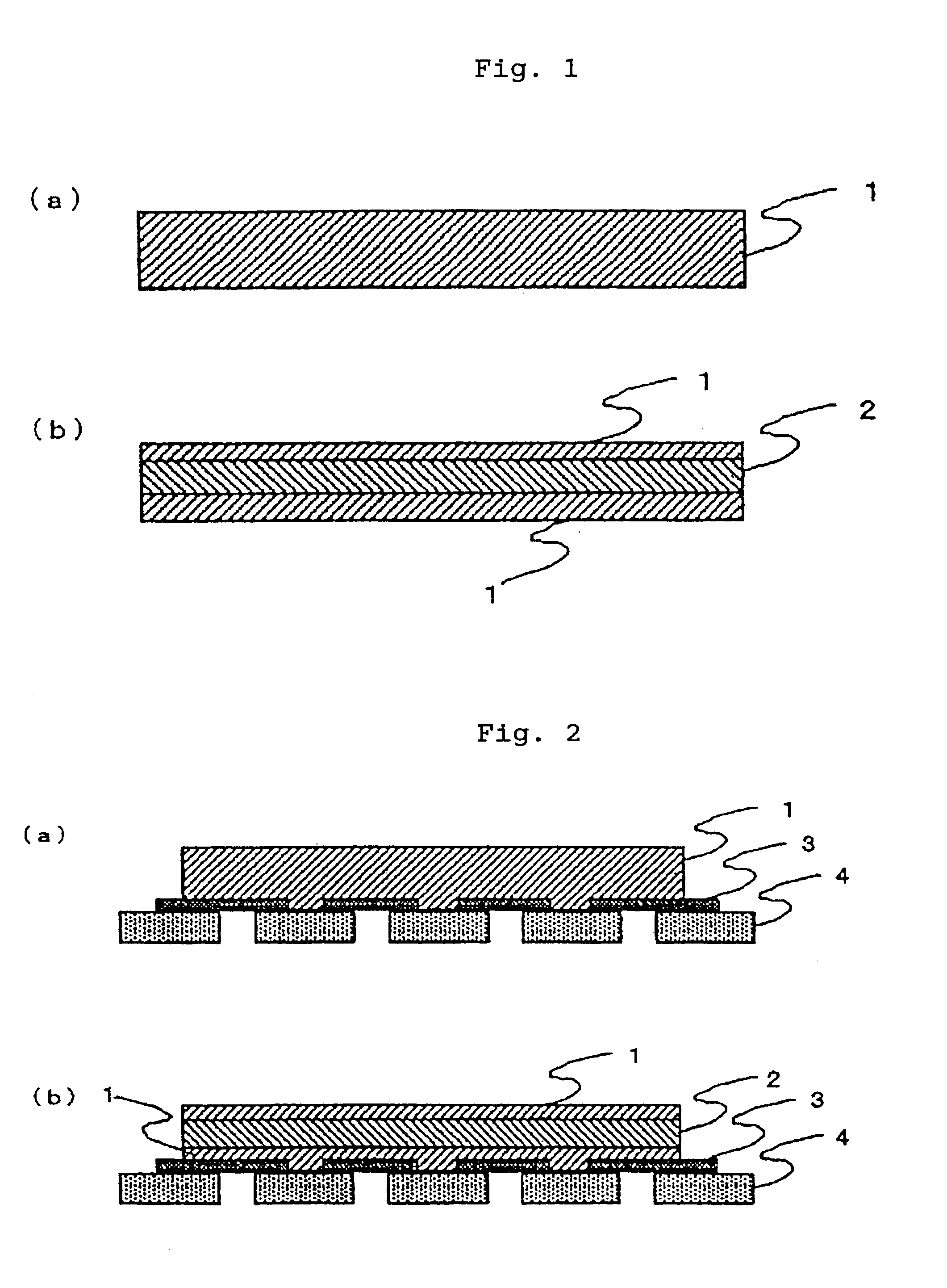
An adhesive film bearing a carrier film was produced by applying adhesive varnish 1 onto a release-treated polyethyleneterephthalate film of 75 .mu.m thick and drying with heat at 140.degree. C. for 5 minutes to form a 75 .mu.m-thick coating of a B-stage state. Two sheets of the adhesive film were stuck together by using a hot roll laminator at a temperature of 110.degree. C., at a pressure of 0.3 MPa and at a rate of 0.3 m / min., to give an adhesive member in a form of a single-layer film of 150 .mu.m thick.

The curing degree of the adhesive in the above-described state was determined by using a DSC (a 912-type DSC produced by E. I. DuPont de Nemours and Company) (heating rate: 10.degree. C. / min.) to be such that it had generated 20% of the heat to be generated by complete curing. The residual solvent content of the adhesive alone was determined to be 1.5 wt. % based on the change in weight before and after heating at 120.degree. C. for 60 minutes.

example 2

An adhesive member in a form of a single-layer film was produced in the same manner as in Example 1, except that adhesive varnish 1 was replaced by adhesive varnish 2.

The curing degree of the adhesive in the above-described state was determined by using a DSC (a 912-type DSC produced by E. I. DuPont de Nemours and Company) (heating rate: 10.degree. C. / min.) to be such that it had generated 20% of the heat to be generated by complete curing. The residual solvent content was 1.4 wt. %.

example 3

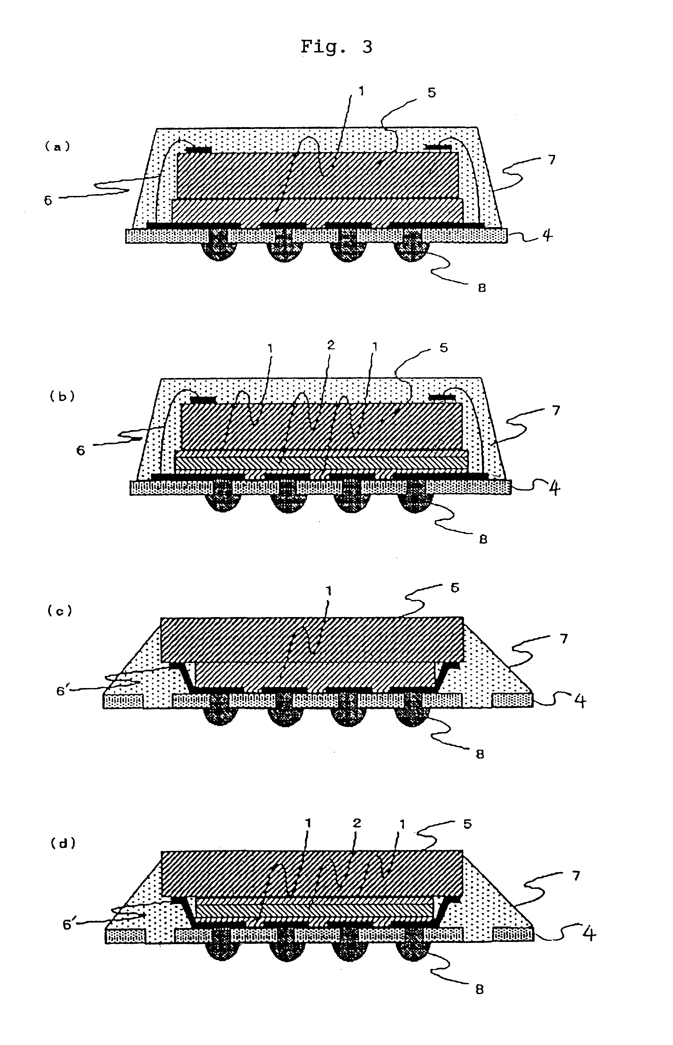
Adhesive varnish 2 was applied onto a 25 .mu.m-thick polyimide film (trade name: UPILEX SGA-25 produced Ube Industries, Ltd.) and dried with heat at 120.degree. C. for 5 minutes to form a 50 .mu.m-thick coating of a B-stage state. The same varnish was then applied onto the polyimide film on the side bearing no adhesive layer and dried with heat at 140.degree. C. for 5 minutes to form a 70 .mu.m-thick coating of a B-stage state, to give an adhesive member comprising the polyimide film used as a core material bearing an adhesive layer on each side.

The curing degree of the adhesive in the above-described state was determined by using a DSC (a 912-type DSC produced by E. I. DuPont de Nemours and Company) (heating rate: 10.degree. C. / min.) to be such that it had generated in the 50 .mu.m-thick layer 25% of the heat to be generated by complete curing, and in the 75 .mu.m-thick layer, 20%. The adhesive in both layers had residual solvent contents of 1.3 to 1.6 wt. %.


PUM

PropertyMeasurementUnit
softening temperatureaaaaaaaaaa
heat resistanceaaaaaaaaaa
storage modulusaaaaaaaaaa

Abstract

An adhesive which comprises (1) 100 parts by weight of an epoxy resin and a hardener therefor, (2) 75 to 300 parts by weight of an epoxidized acrylic copolymer having a glycidyl (meth)acrylate unit content of 0.5 to 6 wt. %, a glass transition temperature of -10° C. or higher and a weight average molecular weight of 100,000 or more and (3) 0.1 to 20 parts by weight of a latent curing accelerator; an adhesive member having a layer of the adhesive; an interconnecting substrate for semiconductor mounting having the adhesive member; and a semiconductor device containing the same.

Description

The present invention relates to an adhesive, an adhesive member, an interconnecting substrate for semiconductor mounting having the adhesive member, and a semiconductor device comprising a semiconductor chip and an interconnecting substrate bonded together by using the adhesive member.With the progress of electronic and electric equipment in recent years, the mounting density of electronic parts has been increased, and new packaging methods have becoming to be used, such as so-called chip scale packages or chip size packages (hereinafter, they will be referred to as CSP) with sizes nearly equal to semiconductor chips, and bare chip packaging.Reliability is one of the most important characteristics requisite for packaging substrates mounted with various electronic parts, such as semiconductor elements. Particularly, connection reliability against thermal fatigue is very important because it directly affects the equipment containing the packaging substrates.One of the causes for the ...

Claims


Application Information

Patent Timeline
Patent Type & Authority Patents(United States)
IPC IPC(8): C08G59/68C08G59/34C09J163/00C09J7/02C08G59/00H01L21/02H01L23/12H01L23/14H01L21/58H05K3/34C08K5/00C08L63/00C09J7/22C09J7/26C09J7/35C09J133/00C09J133/06H01L21/52H05K3/32
CPCC08G59/027C08G59/686C09J7/0203C09J7/0242C09J7/0289C09J133/068C09J163/00H01L24/29H01L24/32H01L24/83C08L63/00C09J2203/326C09J2427/006C09J2433/00C09J2463/00C09J2477/006C09J2479/086C09J2481/006H01L2224/16H01L2224/2919H01L2224/32225H01L2224/48091H01L2224/48227H01L2224/73265H01L2224/8319H01L2224/83855H01L2224/92247H01L2924/01005H01L2924/01012H01L2924/01013H01L2924/01015H01L2924/0102H01L2924/01027H01L2924/01029H01L2924/01033H01L2924/0104H01L2924/01051H01L2924/01058H01L2924/01077H01L2924/01082H01L2924/07802H01L2924/15311H01L2224/29H01L2924/01006H01L2924/01087H01L2924/014H01L2924/0665H01L2224/29101Y10S428/901H01L2924/00013H01L2224/2929H01L2224/29386H01L2924/00011Y10T428/287Y10T428/2891C08L2666/02C08L2666/04C08L2666/22H01L2924/00014H01L2924/00H01L2924/05432H01L2924/05442H01L2924/0532H01L2924/05032H01L2924/0503H01L2924/3512H01L2224/29099H01L2224/29199H01L2224/29299H01L2224/29298H01L2924/351H01L2924/15787H01L2924/181H01L2224/50H01L2224/05573H01L2224/05548H01L2924/15183C09J7/35C09J7/22C09J7/26Y10T428/31511H01L2224/02377H01L2224/2612H01L2924/00012H01L2224/05599
Inventor TANAKA, YUKOSHIMADA, YASUSHIINADA, TEIICHIKURIYA, HIROYUKIYAMAMOTO, KAZUNORIKUMASHIRO, YASUSHISUMIYA, KEIJI
Owner RESONAC CORPORATION
Why Eureka
Try Eureka