Thin film transistors and semiconductor device

a technology of thin film transistors and semiconductor devices, applied in semiconductor devices, semiconductor/solid-state device details, electrical apparatus, etc., can solve the problems of difficult to obtain temperature and treatment time are not necessarily suitable, and achieve the effect of achieving homogeneous crystals over a wide area

Inactive Publication Date: 2004-02-10
SEMICON ENERGY LAB CO LTD
View PDF39 Cites 48 Cited by
  • Summary
  • Abstract
  • Description
  • Claims
  • Application Information

AI Technical Summary

Benefits of technology

The metal element that is added is one or more of those selected from Fe, Co, Ni, Ru, Rh, Pd, Os, Ir, Pt, Cu and Au. The amorphous silicon film to which the metal element is added is heat-treated to thereby form a compound (silicide compound) of silicon with the metal element. This compound then diffuses to assist the crystallization. Germanium that is added to the amorphous silicon does not react with this compound but stays in the peripheries thereof to build up local strain. The strain works to increase the critical radius of the formation of nuclei and, hence, to decrease the density of the formation of nuclei. The strain further limits the orientation of crystals.
When the amorphous semiconductor film is crystallized, the volume of the film contracts due to the rearrangement of atoms if viewed macroscopically. As a result, tensile stress occurs in the crystalline semiconductor film formed on the substrate. Upon containing germanium having an atomic radius larger than that of silicon at a concentration of 0.1 to 10 atomic %, preferably, 1 to 3 atomic %, however, the contraction of volume due to the crystallization is suppressed, and a small internal stress occurs. That is, upon containing germanium at a concentration as contemplated by this invention, the strain in the crystalline semiconductor film can be relaxed.

Problems solved by technology

The above treating temperature and the treating time are not necessarily suitable from the standpoint of productivity of the TFTs.
When a liquid crystal display device is taken into consideration as an applied product using TFTs, a heating furnace of a large size is necessary to cope with an increase in the area of the substrate, not only consuming energy in large amounts in the steps of production but also making it difficult to obtain homogeneous crystals over a wide area.
In the case of the laser treatment, it is difficult to obtain homogeneous crystals due to the lack of stability in the output of the laser oscillator.
Dispersion in the quality of crystals could become a cause of dispersion in the TFT characteristics, and deteriorates the quality of display of the liquid crystal display devices and the EL display devices.
In the crystalline silicon film formed by the above conventional methods, however, the planes of crystalline azimuth exist in a random fashion, and the ratio of orientation is low for particular crystalline azimuths.
That is, since the carriers are scattered and trapped, a TFT having a high electric-field mobility cannot be expected despite the TFT is fabricated by using the above crystalline semiconductor film.
Besides, since the crystalline grain boundaries exist in a random fashion, it is difficult to form the channel-forming region using crystalline particles having a particular crystalline azimuth, and electric characteristics of the TFT tend to become dispersed.
The strain further limits the orientation of crystals.
When germanium is added in amounts larger than the above range, nuclei are formed spontaneously and conspicuously (crystalline nuclei that are not dependent upon the compound of the added metal element) as an alloy of silicon and germanium, making it difficult to increase the ratio of orientation of the obtained crystalline semiconductor film.
When germanium is added in too small amounts, strain does not build up to a sufficient degree making it difficult to increase the ratio of orientation, either.

Method used


Image

  • Thin film transistors and semiconductor device
  • Thin film transistors and semiconductor device
  • Thin film transistors and semiconductor device

Examples


embodiment 1

[Embodiment 1]

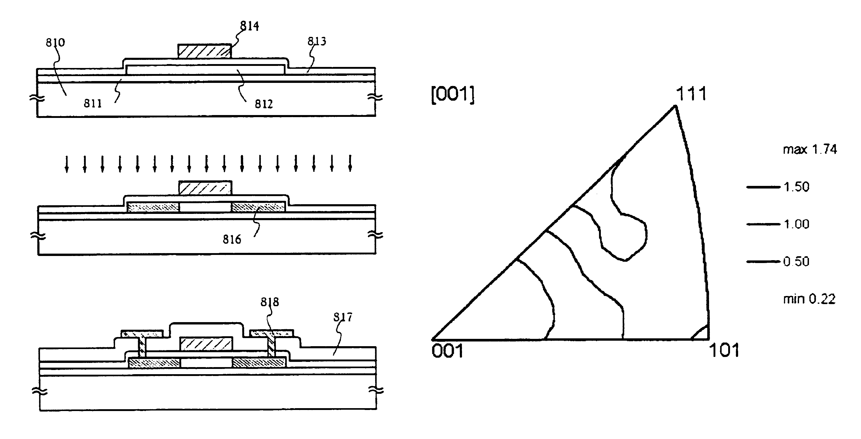
The method of forming the crystalline semiconductor film described with reference to FIGS. 7A-7D are the one that executes the crystallization by adding a metal element into the whole surface of the amorphous silicon film containing germanium to assist the crystallization of silicon. Referring to FIG. 7A, first, the glass substrate 701 is the one represented by the # 1773 glass substrate of Coning Co. On the surface of the substrate 701, there is formed, as a blocking layer 702, a silicon nitride oxide film by using SiH.sub.4 and N.sub.2 O by the plasma CVD method maintaining a thickness of 100 nm. The blocking layer 702 is formed so that alkali metals contained in the glass substrate will not diffuse into the semiconductor film formed thereon.

The amorphous silicon film 703 containing germanium is formed by the plasma CVD method, and is deposited on the substrate 701 by the glow-discharge decomposition while introducing the GeH.sub.4 gas diluted into 10% with SiH.sub.4...

embodiment 2

[Embodiment 2]

Germanium can be added to the amorphous silicon film not only by the method of forming the film by using gases containing elements as represented by SiH.sub.4 and GeH.sub.4 by the plasma CVD method but also by a method of adding germanium by the ion injection method or the ion-doping method (or is also called plasma-doping method) after the amorphous silicon film has been formed. In the plasma CVD method, GeH.sub.4 is preferentially decomposed with the same high-frequency electric power due to a difference in the dissociation energy between SiH.sub.4 and GeH.sub.4. In this case, unless the film-forming conditions are precisely controlled such as employing pulse discharge, a cluster of germanium is formed in the amorphous silicon film making it difficult to uniformly disperse germanium.

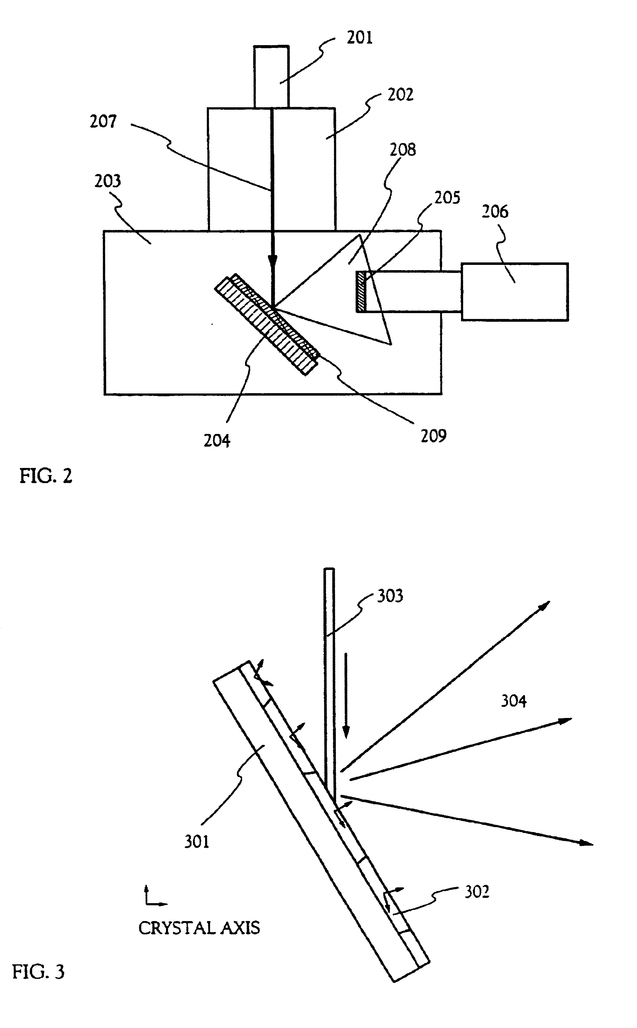
FIGS. 8A and 8B are diagrams illustrating the steps of adding germanium by the ion injection method or the ion-doping method. In FIG. 8A, a blocking layer 702 is formed on a glass substra...

embodiment 3

[Embodiment 3]

Described below with reference to FIGS. 9A-9C is a method of selectively forming the metal element that assists the crystallization of the amorphous semiconductor film. In FIG. 9A, a substrate 720 is the above-mentioned glass substrate or the quartz substrate. When the glass substrate is used, a blocking layer is formed in the same manner as in Embodiment 1.

An amorphous silicon film 721 containing germanium may be formed by the plasma CVD method like in Embodiment 1, or germanium may be introduced by the ion-injection method or by the ion-doping method as in Embodiment 2. It is also allowable to employ a method of formation by decomposing Si.sub.2 H.sub.6 and GeH.sub.4 at a temperature of 450 to 500.degree. C. by the low pressure CVD method.

Then, a silicon oxide film 722 is formed maintaining a thickness of 150 nm on the amorphous silicon film 721 containing germanium. Though there is no particular limitation on the method of forming the silicon oxide film, the silicon...


PUM

PropertyMeasurementUnit
thicknessaaaaaaaaaa
temperatureaaaaaaaaaa
thicknessaaaaaaaaaa

Abstract

The TFT has a channel-forming region formed of a crystalline semiconductor film obtained by heat-treating and crystallizing an amorphous semiconductor film containing silicon as a main component and germanium in an amount of not smaller than 0.1 atomic % but not larger than 10 atomic % while adding a metal element thereto, wherein an orientation ratio of the lattice plane {101} is not smaller than 20% and the lattice plane {101} has an angle of not larger than 10 degrees with respect to the surface of the semiconductor film, and an orientation ratio of the lattice plane {001} is not larger than 3% and the lattice plane {001} has an angle of not larger than 10 degrees with respect to the surface of the semiconductor film, and an orientation ratio of the lattice plane {001} is not larger than 5% and the lattice plane {111} has an angle of not larger than 10 degrees with respect to the surface of the semiconductor film as detected by the electron backscatter diffraction pattern method.

Description

1. Field of the InventionThis invention relates to thin film transistors using a semiconductor film of crystals that are collected having various azimuths (hereinafter referred to as crystalline semiconductor film) as represented by a polycrystalline silicon film, and a semiconductor device formed by using the above thin film transistors. In particular, the invention relates to a semiconductor film forming a channel-forming region, a source region and a drain region of a thin film transistor and to a semiconductor device mounting the above thin film transistors. In this specification, the semiconductor device refers to devices that work by utilizing semiconductor characteristics as a whole inclusive of display devices as represented by a liquid crystal display device and semiconductor integrated circuits (microprocessors, signal processing circuits and high-frequency circuits).2. Prior ArtThere has been developed a technology for fabricating thin film transistors (hereinafter abbrev...

Claims


Application Information

Patent Timeline
Patent Type & Authority Patents(United States)
IPC IPC(8): H01L21/336H01L29/66H01L21/02H01L29/786
CPCH01L29/66757H01L29/78684H01L29/786
Inventor YAMAZAKI, SHUNPEIMITSUKI, TORUKASAHARA, KENJIASAMI, TAKETOMITAKANO, TAMAESHICHI, TAKESHIKOKUBO, CHIHOARAI, YASUYUKI
Owner SEMICON ENERGY LAB CO LTD
Why Eureka
Try Eureka