Semiconductor Device and Method of Manufacturing the Same

a technology of semiconductors and semiconductors, applied in the field of semiconductor films, can solve the problems of local distortion and the effect of limiting the orientation of crystals, and achieve the effect of reducing internal stress and volume shrinkage accompanied by crystallization

Inactive Publication Date: 2006-11-02
SEMICON ENERGY LAB CO LTD
View PDF33 Cites 15 Cited by
  • Summary
  • Abstract
  • Description
  • Claims
  • Application Information

AI Technical Summary

Benefits of technology

[0012] The present invention has been made to present solutions to those problems, and an object of the present invention is therefore to raise the orientation ratio of a crystalline semiconductor film obtained by crystallizing an amorphous semiconductor film through heat treatment and irradiation of intense light such as laser light, ultraviolet rays, or infrared rays and to provide a semiconductor device whose active region is formed from the crystalline semiconductor film and a method of manufacturing the semiconductor device.
[0015] The element for promoting crystallization is one or more elements selected from the group consisting of Fe, Co, Ni, Ru, Rh, Pd, Os, Ir, Pt, Cu, and Au. The thickness of the amorphous semiconductor film is set to 10 to 100 nm. An amorphous silicon film is doped with the metal element given in the above and subjected to heat treatment to form a compound of silicon and the metal element (silicide). Formation of the compound spreads to advance crystallization. Germanium contained in the amorphous silicon film does not react with this compound and generates local distortion by being present around the compound. This distortion acts to increase the critical radius of nuclear generation and to reduce the nuclear generation density. The distortion also has an effect of limiting orientation of crystals.
[0018] The intermittent electric discharge or pulsed electric discharge as above allows selection of radical species (meaning here atoms or molecules that are electrically neutral and chemically active) in the deposition process of the amorphous semiconductor film, so that a film can be formed from a radical species having a relatively long life period. For example, various radical species and ion species are generated when dissolving SiH4 in an electric discharge space. Radical species repeat generation and extinguishment reactions but electric discharge that is continued steadily keeps the existence proportions of radical species fixed. On the other hand, if there is a period where electric discharge is stopped as in intermittent electric discharge or pulsed electric discharge, only radical species that has longer life period is supplied due to the difference in life period between the radical species and ion species to the film deposition surface and is used to form the film.
[0020] The amorphous semiconductor film loses its volume when crystallized due to rearrangement of atoms. As a result, the polycrystalline semiconductor film on the substrate contains tensile stress. However, the volume shrinkage accompanied crystallization can be limited and the internal stress generated can be reduced by making the amorphous semiconductor film contain germanium with a large atom radius in 0.1 atomic percent or more and 10 atomic percent or less, preferably 1 atomic percent or more and 5 atomic percent or less, with respect to silicon. At this point, germanium is contained preferably in a dispersed state in order to obtain a uniform effect throughout the film.

Problems solved by technology

Germanium contained in the amorphous silicon film does not react with this compound and generates local distortion by being present around the compound.
The distortion also has an effect of limiting orientation of crystals.

Method used


Image

  • Semiconductor Device and Method of Manufacturing the Same
  • Semiconductor Device and Method of Manufacturing the Same
  • Semiconductor Device and Method of Manufacturing the Same

Examples


embodiment 1

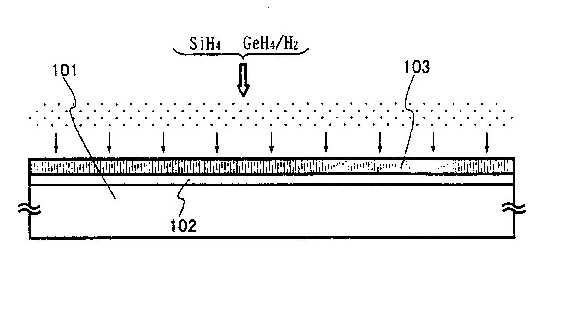
[0095]FIGS. 7A to 7D illustrates a method of forming a crystalline semiconductor film in which an amorphous silicon film containing germanium is crystallized by doping the entire surface of the film with a metal element for promoting crystallization of silicon. In FIG. 7A, a substrate 101 is a glass substrate typical example of which is a Corning # 1737 glass substrate (product of Corning Incorporated). A blocking layer 102 is formed on the surface of the substrate 101 from a silicon oxynitride film with a thickness of 100 nm by plasma CVD using SiH4 and N2O. The blocking layer 102 is provided in order to prevent an alkaline metal contained in the glass substrate from diffusing into a semiconductor film to be formed on the layer.

[0096] An amorphous semiconductor film 103 comprised of silicon and germanium is formed by plasma CVD. GeH4 gas diluted by SiH4 and H2 to 10% is introduced in a reaction chamber and dissolved by glow electric discharge to be deposited on the substrate 101. ...

embodiment 2

[0100] A method of selectively introducing an element for promoting crystallization of an amorphous semiconductor film will be described with reference to FIGS. 8A to 8C. In FIG. 8A, a substrate 120 may be the aforementioned glass substrate or a quartz substrate. When the glass substrate is employed, a blocking layer is formed as in Embodiment 1.

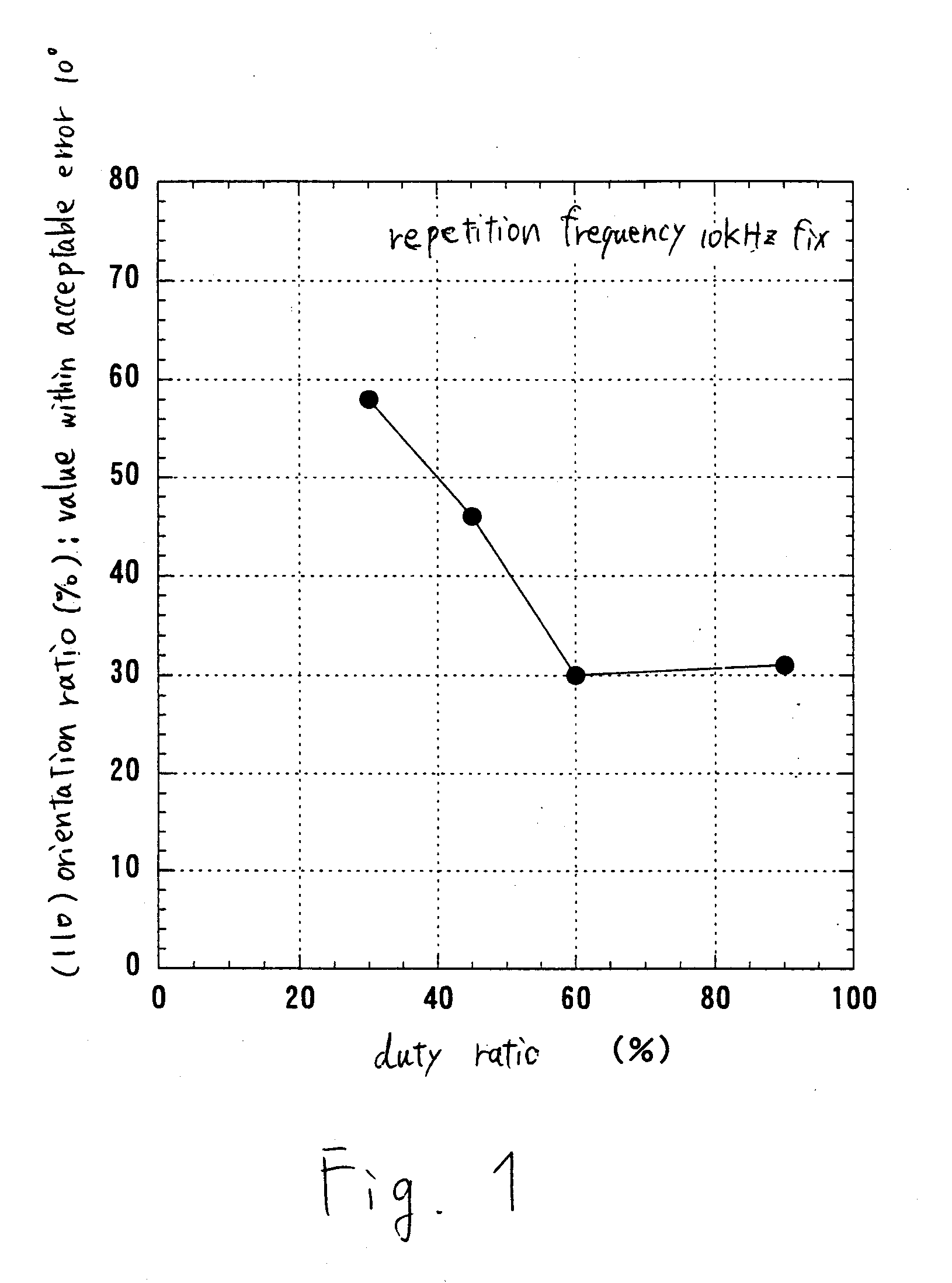
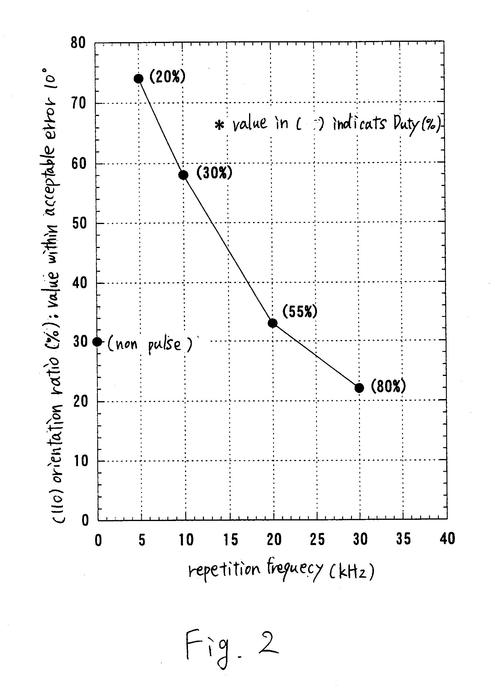
[0101] An amorphous semiconductor film 121 comprised of silicon and germanium is formed by plasma CVD using intermittent electric discharge or pulsed electric discharge as in Embodiment 1.

[0102] A silicon oxide film 122 with a thickness of 150 nm is formed on the amorphous semiconductor film 121 comprised of silicon and germanium. The method of forming the silicon oxide film is not limited. For example, the film is formed through electric discharge in which a mixture of tetraethyl ortho silicate (TEOS) and O2 is used, the reaction pressure is set to 40 Pa, the substrate temperature is set to 300 to 400° C., and the high frequency (13.56 MH...

embodiment 3

[0105] The crystalline semiconductor film formed in accordance with the method described in Embodiment 1 or 2 still has the element that has been utilized in crystallization, typically, nickel. Although not distributed in the film uniformly, the element remains in a concentration over 1×10¹⁹ atoms / cm3 on the average. The film in this state can be used for a TFT and a channel formation region of other various semiconductor devices, of course, but it is preferred to remove the element from the film by gettering.

[0106] This embodiment describes an example of the gettering method with reference to FIGS. 9A to 9C. In FIG. 9A, the glass substrate of Embodiment 1 or a quartz substrate is employed as a substrate 130. When the glass substrate is used, a blocking layer is formed similar to Embodiment 1. A crystalline semiconductor film 131 is formed by the method described in Embodiment 1 or the method described in Embodiment 2. On the surface of the crystalline semiconductor film 131, a sil...


PUM


Abstract

The orientation ratio of a crystalline semiconductor film obtained by crystallizing an amorphous semiconductor film through heat treatment and irradiation of intense light such as laser light, ultraviolet rays, or infrared rays is enhanced, and a semiconductor device whose active region is formed from the crystalline semiconductor film and a method of manufacturing the semiconductor device are provided. In a semiconductor film containing silicon and germanium as its ingredient and having a crystal structure, the {101} plane reaches 30% or more of all the lattice planes detected by Electron backscatter diffraction. This semiconductor film is obtained by forming an amorphous semiconductor film containing silicon and germanium as its ingredient through plasma CVD in which hydride, fluoride, or chloride gas of a silicon atom is used, the repetition frequency is set to 10 kHz or less, and the duty ratio is set to 50% or less for intermittent electric discharge or pulsed electric discharge, and introducing an element for promoting crystallization of the amorphous semiconductor film to the surface thereof to crystallize the amorphous semiconductor film while utilizing the introduced element.

Description

BACKGROUND OF THE INVENTION [0001] 1. Field of the Invention [0002] The present invention relates to a semiconductor film having a polycrystal structure in which crystals mass with diverse orientations as in a polycrystalline semiconductor film. The invention also relates to a semiconductor device whose active region is formed of this semiconductor film and to a method of manufacturing the semiconductor device. In particular, the present invention is suitable for a method of manufacturing a thin film transistor formed a channel formation region in this semiconductor film. The term semiconductor device herein refers to a semiconductor device in general which utilizes semiconductor characteristics to function, and semiconductor integrated circuits, electro-optical devices, and electronic equipment mounted with the semiconductor integrated circuits or the electro-optical devices fall within this category. [0003] 2. Description of the Related Art [0004] A technique has been developed fo...

Claims


Application Information

Patent Timeline
Patent Type & Authority Applications(United States)
IPC IPC(8): H01L21/84H01L21/20H01L21/336H01L21/77H01L27/12H01L29/04H01L29/786
CPCH01L21/0237H01L2029/7863H01L21/02422H01L21/02532H01L21/02609H01L21/02667H01L21/02672H01L21/02675H01L27/12H01L29/04H01L29/045H01L29/66757H01L29/78621H01L29/78666H01L29/78684H01L27/1277H01L27/1285H01L21/0242
Inventor ASAMI, TAKETOMIICHIJO, MITSUHIROTORIUMI, SATOSHIOHTSUKI, TAKASHIMITSUKI, TORUKASAHARA, KENJITAKANO, TAMAEKOKUBO, CHIHOYAMAZAKI, SHUNPEISHICHI, TAKESHI
Owner SEMICON ENERGY LAB CO LTD
Why Eureka
Try Eureka