Thin film transistor and method of manufacturing the same

a technology of thin film transistor and manufacturing method, which is applied in the direction of transistors, semiconductor devices, electrical equipment, etc., can solve the problems of reducing productivity, increasing production costs, and deteriorating reliability of

Inactive Publication Date: 2004-03-16
SAMSUNG DISPLAY CO LTD
View PDF9 Cites 22 Cited by
  • Summary
  • Abstract
  • Description
  • Claims
  • Application Information

AI Technical Summary

Benefits of technology

To overcome the problems described above, preferred embodiments of the present invention provide a thin film transistor (TFT) having a high electric field mobility.
It is another object of the present invention to provide a TFT having a high productivity.

Problems solved by technology

However, the conventional method of manufacturing the TFT using the MILC technique additionally requires a mask process to form the offset regions 17, thereby lowering productivity and increasing the production costs.
In addition, an MILC front 11F, including a metal silicide, exists in the channel area 11C and serves as a defect of the TFT, thereby deteriorating reliability of the TFT.
However, this method has a problem in that a crystallization is non-symmetrically performed and thus a processing time for crystallization is increased.

Method used


Image

  • Thin film transistor and method of manufacturing the same
  • Thin film transistor and method of manufacturing the same
  • Thin film transistor and method of manufacturing the same

Examples


Embodiment Construction

Reference will now be made in detail to preferred embodiments of the present invention, an example of which is illustrated in the accompanying drawings.

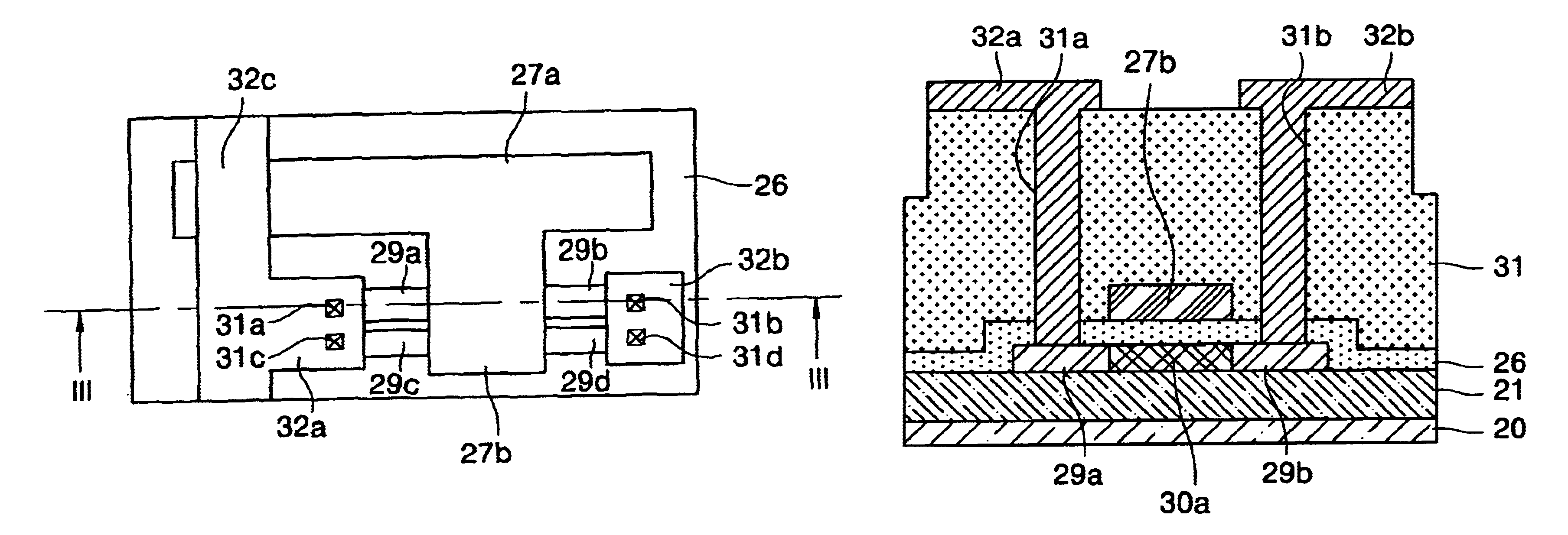
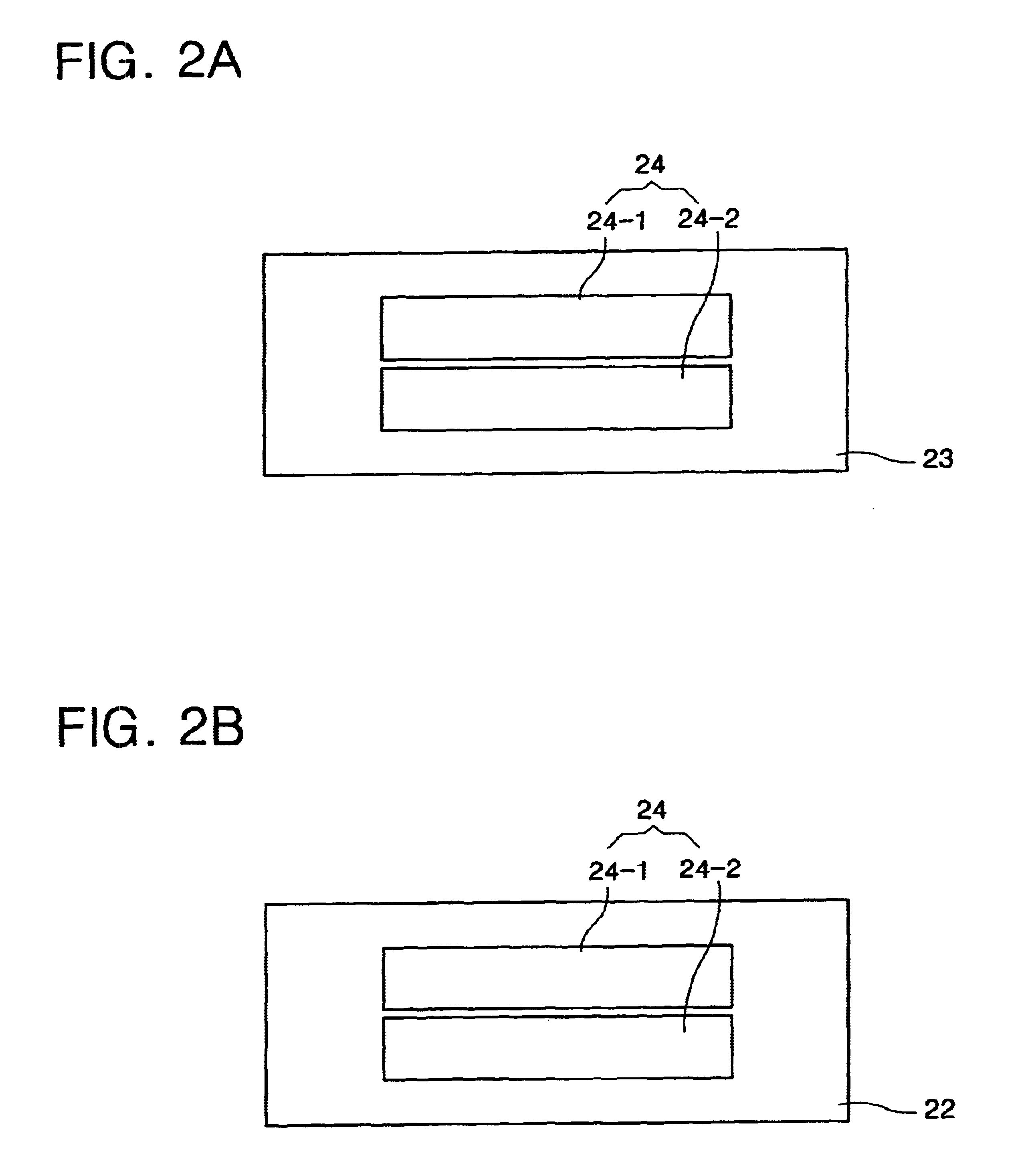
Referring to FIGS. 2A and 3A, a buffer layer 21, an amorphous silicon layer 22 and a blocking layer 23 are sequentially formed on an insulating substrate 20. The buffer layer 21 is preferably made of an oxide layer and serves to prevent an impurity from being diffused into a semiconductor layer which will be formed in a subsequent process. The blocking layer 23 is preferably made of an oxide layer.

There are two methods to form the buffer layer 21, the amorphous silicon layer 22, and the blocking layer 23. A first method is that after the buffer layer 21 is formed on the insulating substrate 20, the amorphous silicon layer 22 and the blocking layer 23 are deposited using a plasma-enhanced chemical vapor deposition (PECVD) technique. The second method is that the buffer 21, the amorphous silicon layer 22, and the blocking layer 23 can ...


PUM


Abstract

A method of manufacturing a thin film transistor that provides high electric field mobility is disclosed. The method comprising: a) forming an amorphous silicon layer and a blocking layer on an insulating substrate; b) forming a photoresist layer having first and second photoresist patterns on the blocking layer, the first and second photoresist patterns spaced apart from each other; c) etching the blocking layer using the first photoresist pattern as a mask to form first and second blocking patterns; d) reflowing the photoresist layer, so that the first and second photoresist patterns abut on each other to entirely cover the first and second blocking patterns; e) forming a metal layer over the entire surface of the insulating substrate; f) removing the photoresist layer to expose the blocking layer and an offset region between the blocking layer and the metal layer; g) crystallizing the amorphous silicon layer to form a poly silicon layer, wherein a portion of the amorphous silicon layer directly contacting the first metal layer is crystallized through a metal induced crystallization (MIC), and the remaining portion of the amorphous silicon layer is crystallized through a metal induced lateral crystallization (MILC), so that a MILC front exists on a portion of the poly silicon layer between the first and second blocking patterns; h) etching the poly silicon layer using the first and second blocking patterns as a mask to form first and second semiconductor layers and to remove the MILC front; and i) removing the first and second blocking patterns.

Description

1. Field of the InventionThe present invention relates to a thin film transistor and a method of manufacturing the same, and, more particularly, to a thin film transistor manufactured according to a method that provides high electrified mobility, high reliability and simplified manufacturing.2. Description of Related ArtA poly silicon layer is generally used as a semiconductor layer of a thin film transistor (TFT). The poly silicon layer is formed such that an amorphous silicon layer is first deposited on a substrate and crystallized at a predetermined temperature. A method of crystallizing the amorphous silicon layer includes an eximer laser annealing (ELA) technique, a solid phase crystallization (SPC) technique, and a metal induced lateral crystallization (MILC) technique.Of these techniques, the MILC technique is disclosed in U.S. Pat No. 6,097,037 and has an advantage in that the amorphous silicon layer is crystallized at a relatively low temperature and at a relatively short p...

Claims


Application Information

Patent Timeline
Patent Type & Authority Patents(United States)
IPC IPC(8): H01L21/336H01L29/66H01L21/02H01L29/786
CPCH01L29/66757H01L29/78696H01L29/786
Inventor SO, WOO-YOUNG
Owner SAMSUNG DISPLAY CO LTD
Why Eureka
Try Eureka