Sputter apparatus for producing multi-component metal alloy films and method for making the same

Inactive Publication Date: 2004-03-23
NOVELLUS SYSTEMS
View PDF12 Cites 77 Cited by
  • Summary
  • Abstract
  • Description
  • Claims
  • Application Information

AI Technical Summary

Benefits of technology

It is another object of the present invention to provide a planar target or a hollow cathode magnetron target that allows for a very high magnesium content to produce high-magnesium CuMg films, typically having a magnesium atomic percentage greater than about four.
It is yet another object of the present invention to provide a sputter apparatus in which the areal percent of the target metal alloy can

Problems solved by technology

A disadvantage of planar magnetrons in which the target is essentially a flat surface is that the magnetic field lines must pass uniformly through the entire target.
This makes uniform sputtering of the planar target extremely difficult.
Problems arise when different combinations of metal alloys are required for deposition.
Fabrication of a CuMg alloy target is problematic since the hardness of a CuMg alloy increases greatly when the magnesium concentration exceeds approximately 4 atomic percent.
This makes it impractical to fabricate a high magnesium concentration copper-magnesium target, in either a planar or three-dimensional configuration, e.g., a hollow cathode magnetron (HCM) target.
The first factor concerns the inefficient transport of the sputtered magnesium to the wafer.
Another problem with physical vapor deposition (PVD) is the deposition of a conformal film onto high aspect-ratio features that requires a directional, ionized PVD approach.
Unfortunately, the ioniz

Method used


Image

  • Sputter apparatus for producing multi-component metal alloy films and method for making the same
  • Sputter apparatus for producing multi-component metal alloy films and method for making the same
  • Sputter apparatus for producing multi-component metal alloy films and method for making the same

Examples


Example

)

In describing the preferred embodiment of the present invention, reference will be made herein to FIGS. 1-9 of the drawings in which like numerals refer to like features of the invention.

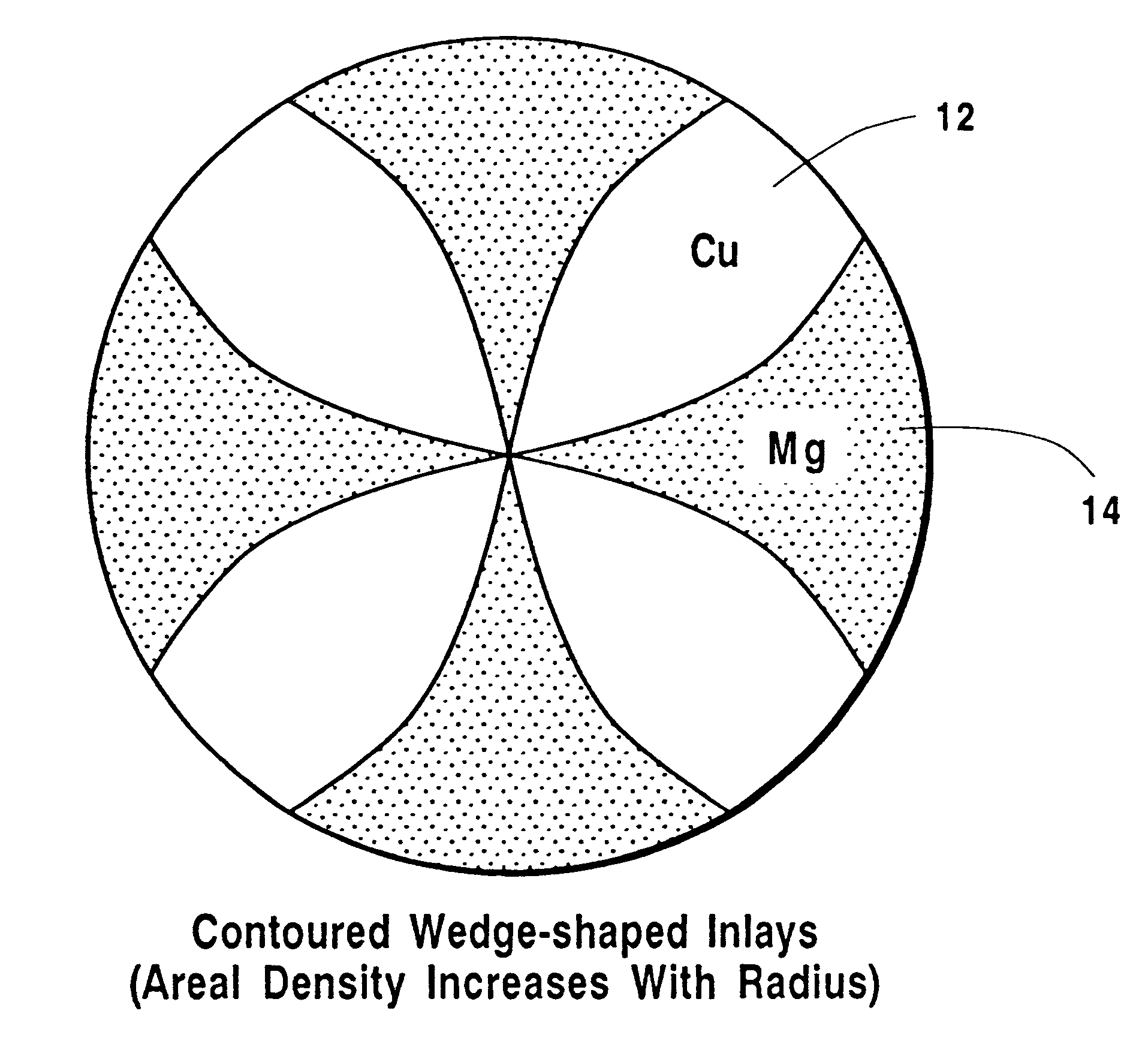
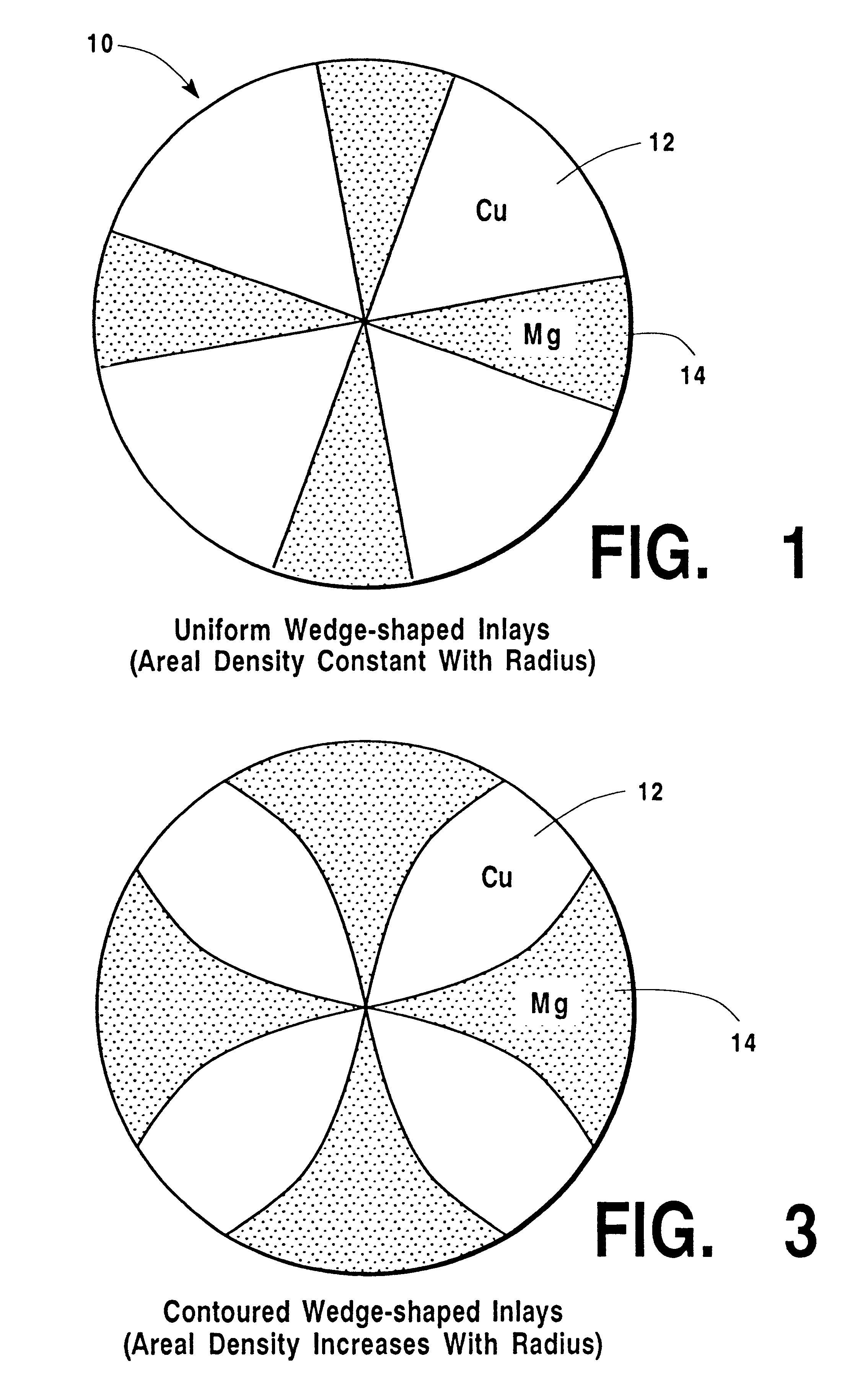
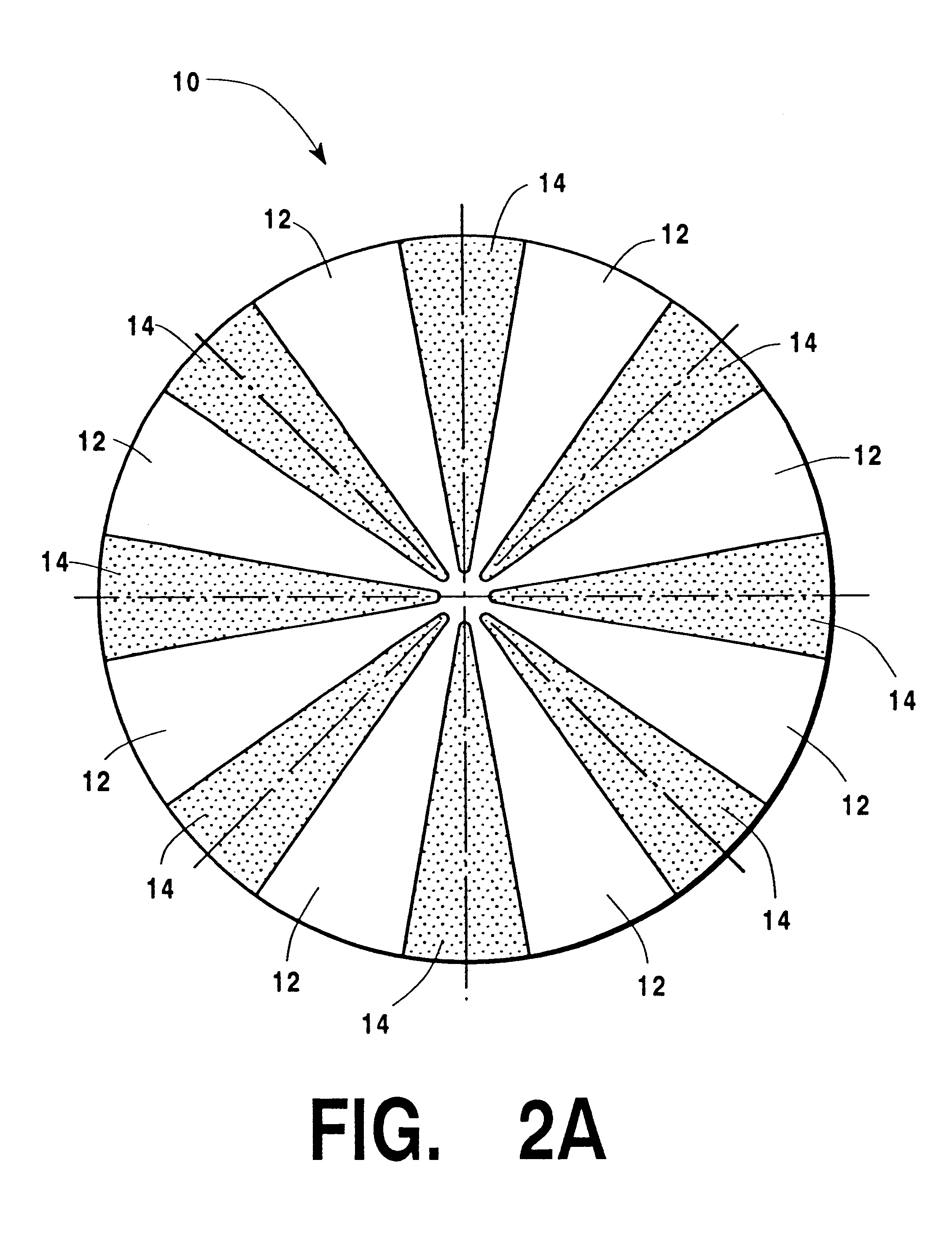
A mosaic or inlaid sputter target design is disclosed that is suitable for conventional planar magnetron deposition, RF ionized physical vapor deposition, HCM ionized PVD, ionized metal plasma (IMP) deposition, or self-ionized plasma (SIP) deposition of multi-component alloys for use in integrated circuit (IC) metallization. By way of an example of immediate interest to the IC community, deposition of binary CuMg alloys is disclosed for the preferred embodiment. However, while the invention is described with respect to targets for CuMg films, it can readily be applied to prepare targets for other alloys, including other copper alloys with similar application and benefit to IC processing, such as CuAl, CuBe, CuB, CuCd, CuCo, CuCr, CuIn, CuPd, CuSn, CuTa, CuTi, CuZr and CuZn. Other non-copper binary ...


PUM

PropertyMeasurementUnit
Densityaaaaaaaaaa
Surface areaaaaaaaaaaa
Semiconductor propertiesaaaaaaaaaa

Abstract

A mosaic or inlaid sputter target design suitable for conventional planar magnetron deposition, RF ionized physical vapor deposition, HCM ionized PVD, ionized metal plasma (IMP) deposition, or self-ionized plasma (SIP) deposition of multi-component alloys for use in integrated circuit metallization. Inlays are inserted within a planar sputter target in the shape of wedges, wires, or buttons to achieve uniform deposition of films on semiconductor substrates during sputtering. Metal alloy strips within a three-dimensional HCM target achieve the same uniform deposition. The deposition leads to the production of CuAl, CuBe, CuB, CuCd, CuCo, CuCr, CuIn, CuPd, CuSn, CuTa, CuTi, CuZr or CuZn alloy films deposited on the wafer. Non-copper films may also be deposited. The inlay-target adjoining surfaces may be machine stepped or tapered to limit wicking from the target backing material.

Description

1. Field of the InventionThe present invention relates to an apparatus for sputtering coatings onto substrate deposition surfaces, particularly to sputtering multi-component metal alloy films onto the substrate, such as a copper-magnesium alloy film having high magnesium content. The invention relates specifically to a magnetron sputter target for use in physical vapor deposition of thin films on semiconductor substrates, and a method for making the same.2. Description of Related ArtThickness uniformity and structural integrity are increasingly important for sputtered coatings in physical vapor deposition processes. Modern sputtering is typically done with magnetron cathodes. In a magnetron cathode, the target erosion rate is highest where the magnetic field is parallel to the target surface. A disadvantage of planar magnetrons in which the target is essentially a flat surface is that the magnetic field lines must pass uniformly through the entire target. However, typically there re...

Claims


Application Information

Patent Timeline
IPC IPC(8): C23C14/34
CPCC23C14/3407H01J37/3429
Inventor KAILASAM, SRIDHAR K.POWELL, RONALD A.SETTLES, E. DERRYCK
Owner NOVELLUS SYSTEMS
Why Eureka
Try Eureka