Field emission display cathode (FED) plate with an internal via and the fabrication method for the cathode plate

a cathode plate and field emission technology, applied in the manufacture of electrode systems, electric discharge tubes/lamps, discharge tubes luminescnet screens, etc., can solve the problems of reducing yield, compromising the vacuum inside the display, and glass frit has a tendency to corruption, so as to increase the evenness and durability of the fed frame

Inactive Publication Date: 2004-06-15
AU OPTRONICS CORP
View PDF19 Cites 12 Cited by
  • Summary
  • Abstract
  • Description
  • Claims
  • Application Information

AI Technical Summary

Benefits of technology

Accordingly, an object of the invention is to provide an FED cathode plate with an internal via, which prevents diffusion of outside air from corrupting the vacuum inside, thus increasing the evenness and durability of the FED frame.

Problems solved by technology

The glass frit, however, has a tendency toward corruption.
Although the chromium can prevent corruption from the glass frit, the adhesion difference between chromium and the SiO.sub.2 composing the dielectric layer 16 can easily cause splits in the edge of the structure during durability testing of the product, compromising the vacuum inside the display.
In such cases, the display provides uneven illumination and a friable structure in the sealed area, thus reducing the yield.
As well, the hole 4 is small, about 1 .mu.m, and the efficient depth of focus (DOF) for photolithography is low, so that exposure uniformity may be insufficient, further causing stepper shots' marks, reducing the yield of the cathode plate.

Method used


Image

  • Field emission display cathode (FED) plate with an internal via and the fabrication method for the cathode plate
  • Field emission display cathode (FED) plate with an internal via and the fabrication method for the cathode plate
  • Field emission display cathode (FED) plate with an internal via and the fabrication method for the cathode plate

Examples


Embodiment Construction

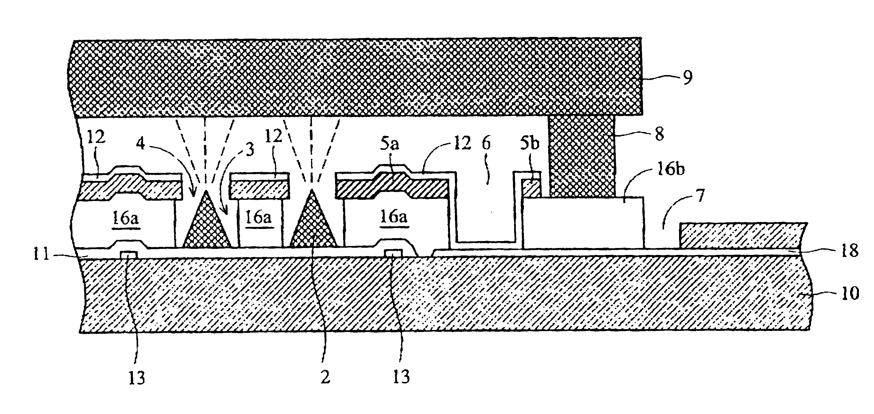
FIG. 3 is a schematic diagram of an FED cathode plate according to the invention. In FIG. 3, in addition to the typical FED structure, the structure also includes an internal via 6; a second dielectric layer 16b, a second gate line 5b, and a metal layer 12 covering the gate lines 5a, 5b and the internal via 6.

As shown in FIG. 3, the FED cathode plate with the internal via has a substrate 10 as the base of deposition. The material of the substrate 10 is glass. The resistive layer 11, a doped layer with a plurality of cathode conductors 13, is implemented over the substrate 10 to prevent a microtip 2 from being formed from excessive current. The material for the cathode conductors is niobium (Nb). The cathode conductors 13 are etched based on a column pattern to create a column line surrounding the cathode conductors 13. At the same time, the tape line 18 is formed on the substrate 10 maintaining a distance from the resistive layer 11. The tape line 18 is chromium (Cr). The tape line ...


PUM


Abstract

an FED cathode plate with internal via includes an internal via; a second dielectric layer; a second gate line; a metal layer 12 covering the gate line and the internal via; and a contact. The internal via is located on a typical tape line. The second dielectric layer is located on the tape line and abutted against the internal via, thereby connecting to an anode by an adhesive. The second gate line is located on the second dielectric layer and abutted against the internal via. The metal layer is covered over the first gate line, the internal via, and the second gate line; and the contact is located on the tape line and connected adjacent to the second dielectric layer, thereby electrically connecting a lead to outside.

Description

BACKGROUND OF THE INVENTION1. Field of the InventionThe invention relates to an FED structure, particularly to an FED cathode plate with an internal via and the fabrication method for the cathode plate, which uses the vaporization to form the internal via such that the cathode sealing area of FED appears homogeneous, thereby increasing the yield.2. Description of the Related ArtFIG. 1 is a schematic diagram of a typical FED cathode plate. In FIG. 1, the FED cathode plate is generally formed by layers successively deposited onto a substrate 10. The layers include a resistive layer 11, a cathode conductor layer 13, a microtip 2, a microtip cavity 3, a microtip hole 4, a gate line 5, a contact 7, a dielectric layer 16, a tape line 18, a seal 8, and an anode plate 9.As shown in FIG. 1, in such a structure, the FED emits electrons induced by the electrical field of the gate line 5 from the microtip 2 through the hole 4. The emitted electrons are conducted and sped up by the anode plate 9...

Claims


Application Information

Patent Timeline
Patent Type & Authority Patents(United States)
IPC IPC(8): H01J29/00H01J29/92H01J1/30
CPCH01J29/92H01J31/127H01J2329/92H01J2329/90
Inventor CHANG, CHIH-CHIN
Owner AU OPTRONICS CORP
Why Eureka
Try Eureka