

Complementary source follower circuit controlled by back bias voltage
a follower circuit and circuit technology, applied in pulse generators, pulse techniques, instruments, etc., can solve the problems of low driving power, increased power consumption, waste of current flow, etc., and achieve high performance and area-efficient
Inactive Publication Date: 2004-07-20
RPX CORP
View PDF12 Cites 17 Cited by
- Summary
- Abstract
- Description
- Claims
- Application Information
AI Technical Summary
Benefits of technology
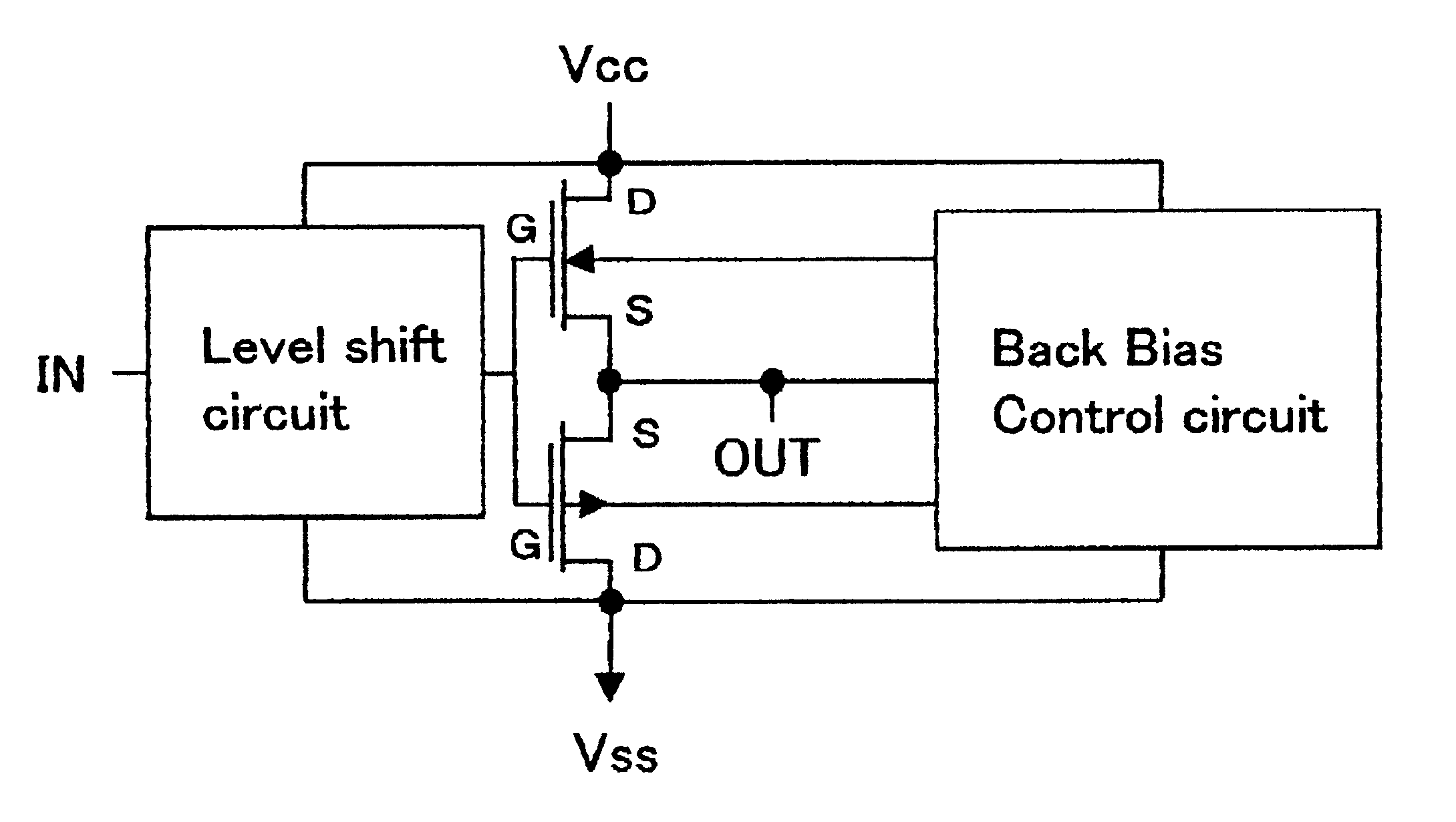
The present invention provides a complementary source follower circuit that can be fabricated using standard MOSFET technology without the need for special manufacturing processes. The circuit has the advantage of being more efficient and reducing power consumption when in stand-by mode. It can also be used in combination with other analog and digital circuits on the same chip without the need for additional devices. The circuit can be designed and fabricated using known CMOS rules and methodologies. The invention also provides a level shift circuit that can be used when the threshold voltage cannot be shifted enough to achieve linearity. Overall, the invention provides a high performance, area-efficient complementary source follower circuit that can be easily integrated into existing CMOS logic technology.
Problems solved by technology
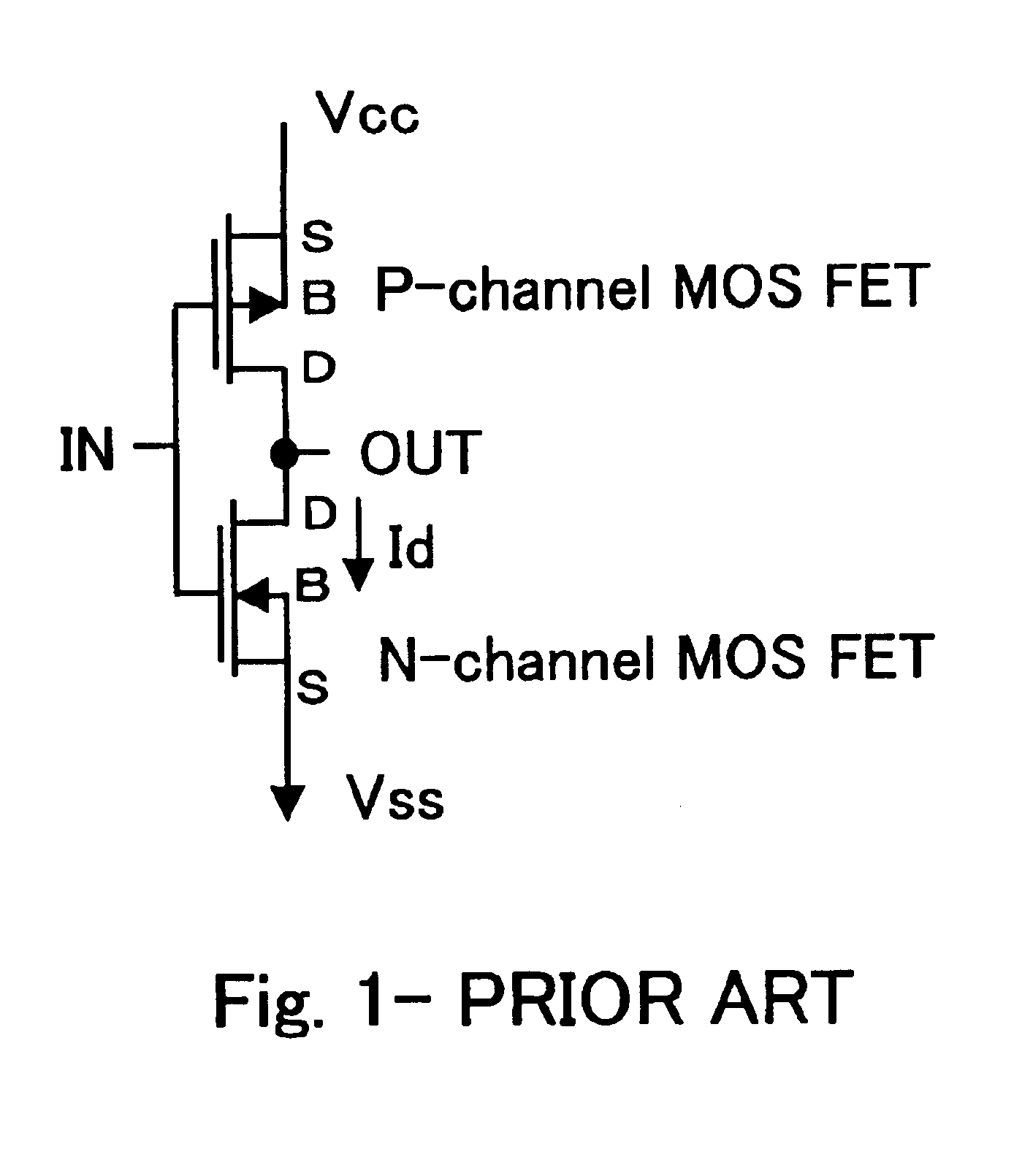
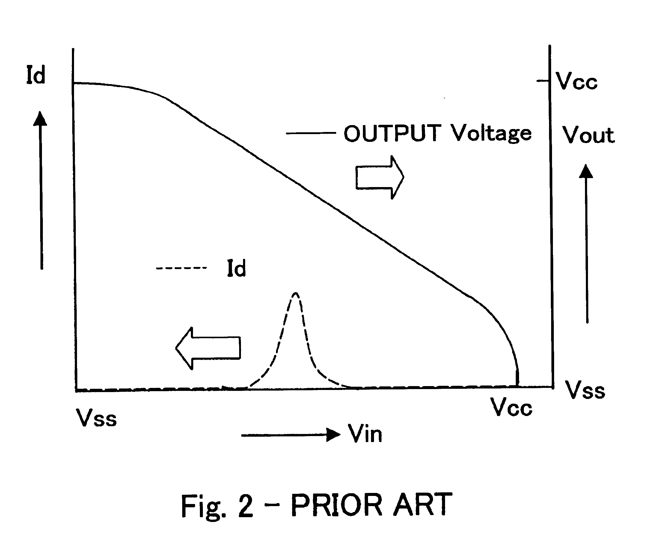
This current flow is wasted power.
But in the circuit of FIG. 6, when the transistor is "on" a current steadily flows between Vcc and Vss, which increases power consumption.
Also, the driving power is low because the current is shared between both the active load and the output load.
However, eliminating the source-to-body connection in FIG. 7 results in non-linearity between the output voltages of the two transistors because the characteristics of the two transistors are not symmetrical.
Method used
View moreImage
Smart ImageViewing Examples

Examples
Embodiment Construction
complementary source follower circuit similar to that of FIG. 11 could have an NFET with a threshold voltage of 0.2 volts and a PFET with a threshold voltage of -0.2 volts, where Vcc is 0.9 volts and Vss is -0.9 volts. The level shift circuit could shift the input voltage of the NFET by -0.3 volts and the input voltage of the PFET by 0.3 volts to eliminate the dead gap. Then, in standby mode, the back bias control circuit could shift the threshold voltage of the NFET by 0.3 volts and the threshold voltage of the PFET by -0.3 volts to re-create a dead gap and reduce Id to zero.
Login to View More PUM
 Abstract
A complementary source follower circuit has an N-channel type transistor and a P-channel transistor. The threshold voltage of each transistor is independently controlled by a back bias voltage control circuit so that the input voltage and the output voltage relationship can be made linear without the use of an additional circuit such as a level shifting circuit. Also, power consumption can be reduced when the circuit is in standby mode by using the back bias voltage control circuit to achieve non-linearity. A back bias voltage control circuit can also be used to control the threshold voltage of a transistor in series with a resistance load to reduce power usage.
Description
BACKGROUND OF INVENTIONThis invention relates to a semiconductor circuit on a large scale integrated circuit(LSI). In particular, it relates to a complementary source follower circuit of a MOS (metal oxide semiconductor) LSI that is suitable for an output buffer of an analog circuit.FIG. 1 shows a conventional CMOS (complementary MOS) drain follower circuit. In FIG. 1, there are two transistors, a P-channel MOSFET (metal oxide semiconductor field effect transistor) and an N-channel MOSFET. Each transistor has a source (S), a drain (D), a gate (G), and a body (B). This circuit can be used to invert signals, i.e., to convert a logical "0" into a logical "1" and a logical "1" into a logical "0," where a logical "0" is represented by the voltage Vss and a logical "1" is represented by the voltage Vcc. The logical "1" or "0" signal is supplied to "IN" and the inverted logical "0" or "1" signal is sent to "OUT." The voltages Vss and Vcc are kept constant during the operation of the circui...
Claims
Login to View More Application Information
Patent Timeline
 Patent Type & AuthorityPatents(United States)
IPC IPC(8): H03K19/00H03K17/0814H03K17/08H03K17/00
CPCH03K17/08142H03K19/0027H03K2217/0018H03K2217/0036
InventorANDO, YOSHIYUKI
OwnerRPX CORP