Wiring board with a waveguide tube and wiring board module for mounting plural wiring boards

a technology of wiring board and waveguide tube, which is applied in the direction of waveguides, waveguide type devices, printed circuit assembling, etc., can solve the problems of whole module defective, increase in the size of the metallic chassis, and introduction of the danger of hermetical sealing being ruined

Inactive Publication Date: 2004-07-27
KYOCERA CORP
View PDF7 Cites 16 Cited by
  • Summary
  • Abstract
  • Description
  • Claims
  • Application Information

AI Technical Summary

Benefits of technology

According to the present invention, terminal ends of the laminated waveguide tubes are exposed at lateral sides of the wiring boards, and with these exposed faces contacted with each other, the wiring boards are surface-mounted on the surface of a module substrate. Accordingly, a high frequency signal of a microwave or a millimeter wave can be transmitted directly from one wiring board to the other wiring board without an intermediary of connection parts of the wiring boards to the module substrate or a wiring layer on the module substrate. This achieves a low loss high frequency transmission between the wiring boards regardless of the dielectric loss tangent and dielectric constant of the module substrate.
Further, an economical module substrate can be used, and mounting the wiring boards on the surface of a module substrate improves productivity. It is therefore possible to obtain a low-cost wiring board module.
Further, according to the present invention, a notch can be formed in both or one of the exposed faces to come in contact with each other, and is filled with adhesives having predetermined dielectric properties. This enhances the bonding properties of the wiring boards, thus further improving the transmission characteristics.

Problems solved by technology

In such a multichip module, a number of high frequency elements are mounted on a single metallic chassis, resulting in an increase in the size of the metallic chassis.
Accordingly, the metallic chassis and the lid are readily deformed, thus introducing the danger of the hermetical sealing being ruined.
Accordingly, even a single defective connection makes the whole module defective.
This adversely affects module production yield.
In such a case, when the signal frequency is high, a high frequency signal reflects at the connection parts of the wiring boards with the wiring layer of the module substrate, thus disadvantageously causing the high frequency signal to be readily attenuated.
Further, when a composite material such as a glass-epoxy resin composite material is used as the material of a module substrate, the dielectric loss tangent which causes a high frequency signal to be adversely attenuated on the surface of the module substrate.
However, when a material small in dielectric loss tangent is used as the module substrate material, the cost becomes extremely expensive.
This may possibly have an adverse effect on the transmission characteristics of the high frequency signal between the wiring boards A2, A2'.

Method used


Image

  • Wiring board with a waveguide tube and wiring board module for mounting plural wiring boards
  • Wiring board with a waveguide tube and wiring board module for mounting plural wiring boards
  • Wiring board with a waveguide tube and wiring board module for mounting plural wiring boards

Examples


Embodiment Construction

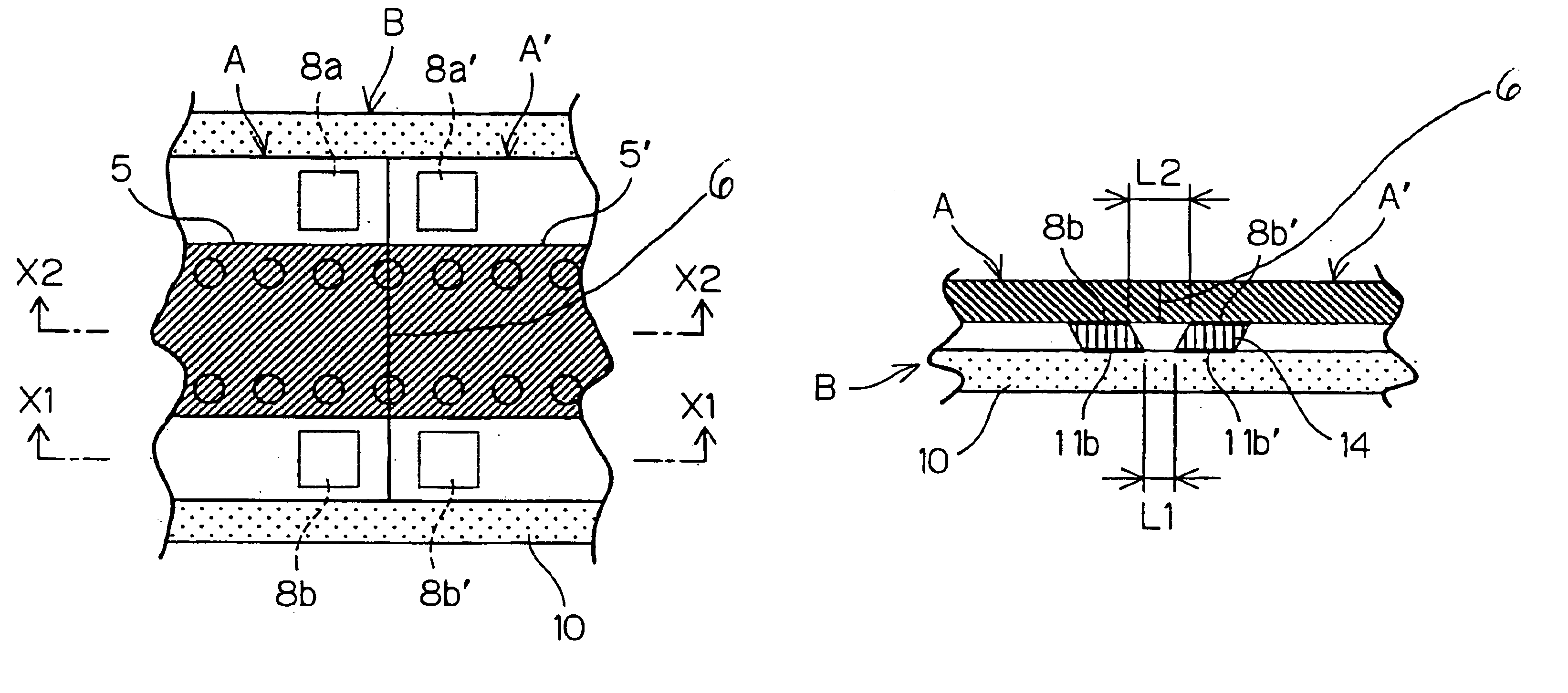
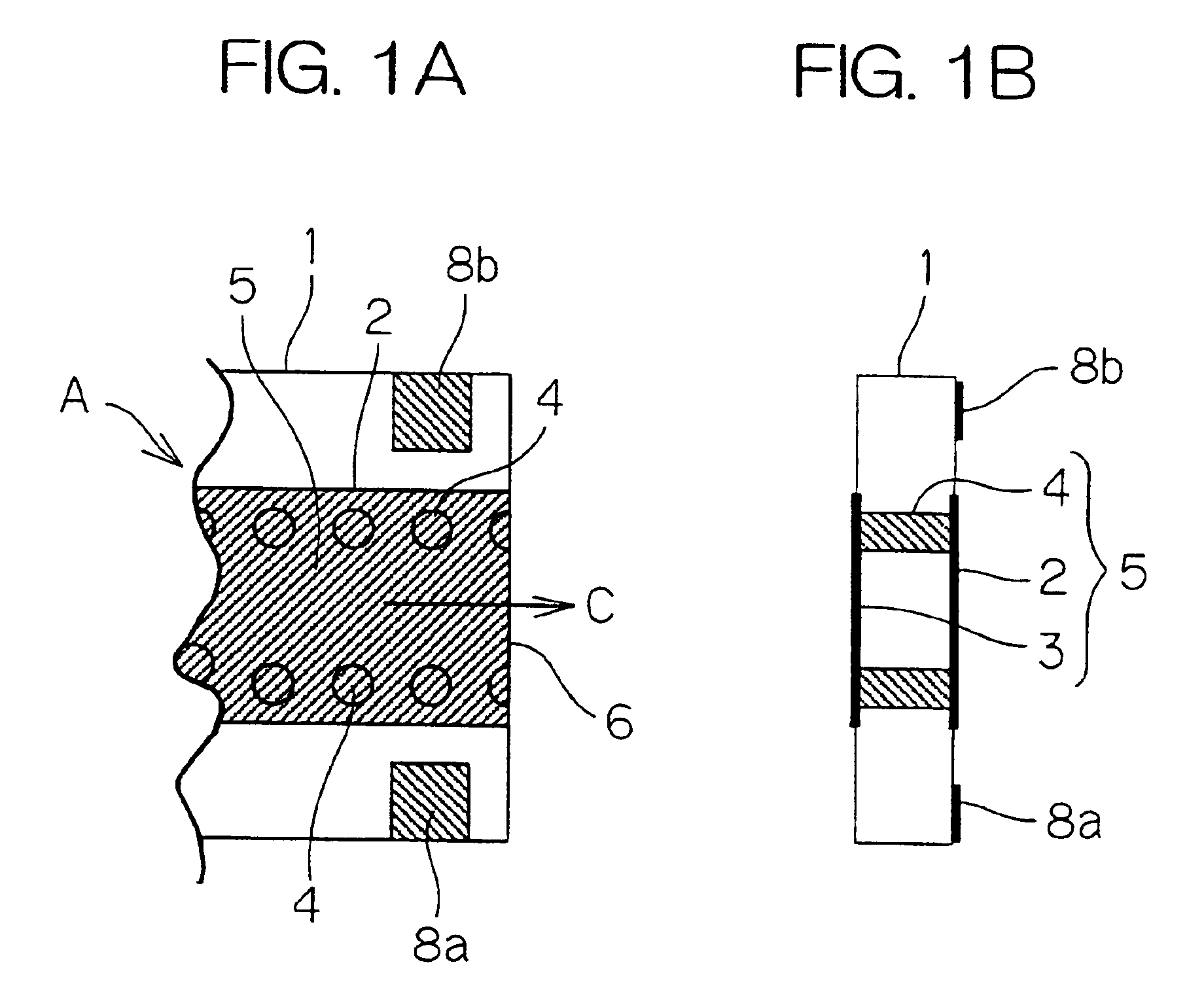
To confirm the operational effect of the present invention, the following tests were conducted. By a usual lamination simultaneous calcining technique, wiring boards as shown in FIGS. 1 and 4 were prepared with the use of a tungsten metalized ink and a green sheet of alumina ceramics of which relative dielectric constant was 9 and dielectric loss tangent was 0.0006 at 10 GHz after calcination. To those exposed faces of the wiring boards which are opposite to the mutual contact faces thereof, metal fittings each having an opening identical with that of a standard waveguide tube WR-1, were brazed with silver solder and then subjected to nickel-gold plating.

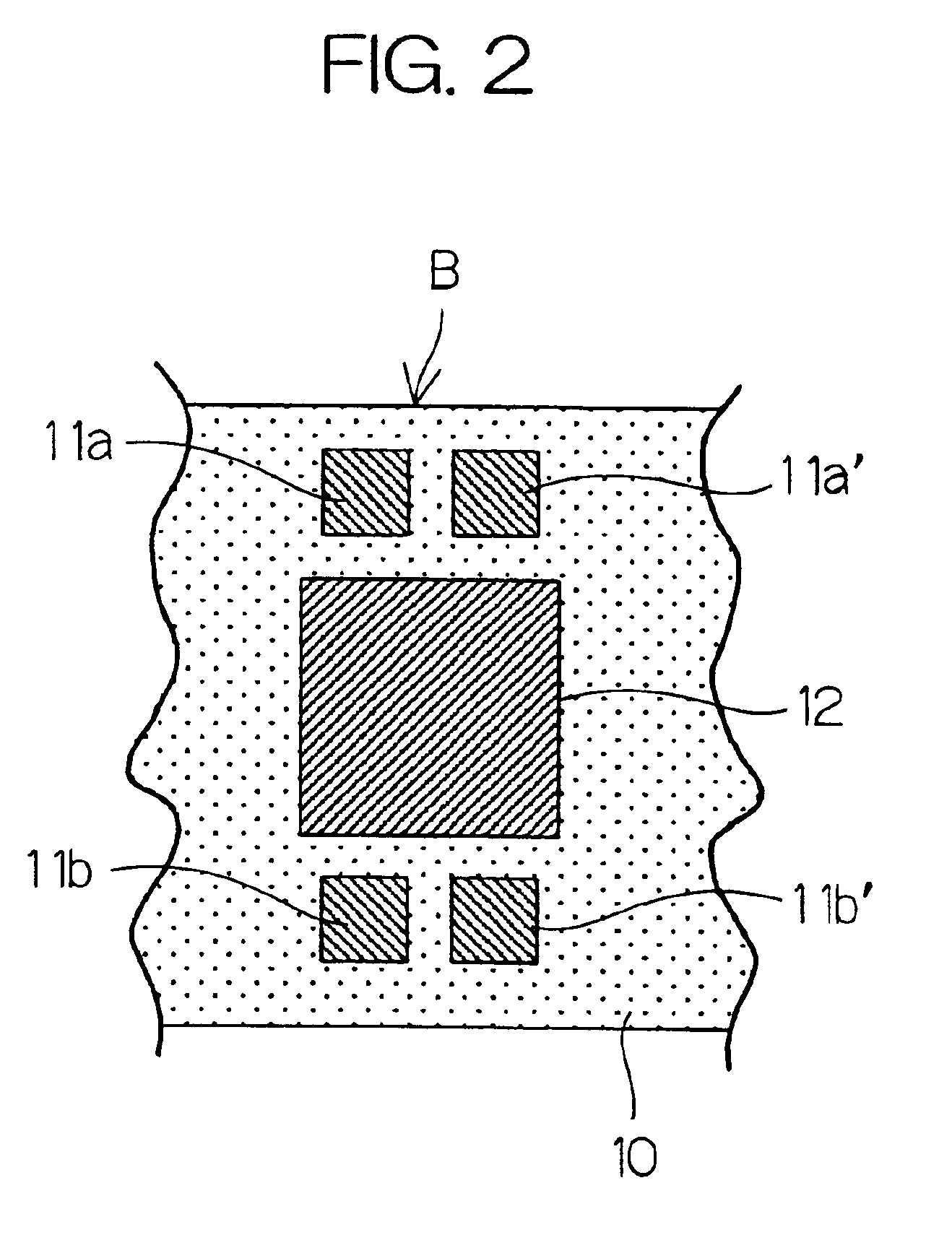
On the other hand, as each module substrate forming an outer circuit board, there was used a print substrate FR-4 which has a conductor pattern as shown in FIG. 2 and which is made of a glass-epoxy resin composite material.

Solder paste of the tin-silver-copper type was printed on the connection pads of the print substrates. With the...


PUM


Abstract

A wiring board module has two wiring boards placed on an external circuit board. In each wiring board, a terminal end of a laminated waveguide tube is exposed at a lateral side of a dielectric substrate, thus forming an exposed face, and the dielectric substrate is provided at the bottom thereof in the vicinity of the exposed face with connection pads to be used for mounting the wiring board on the surface of the external circuit board. The exposed faces of the laminated waveguide tubes of the two wiring boards are contacted with each other, and the connection pads at the bottoms of the wiring boards are connected and fixed to connection pads disposed on the surface of the external circuit board.

Description

This application is based on application No. 200-1083749 filed in Japan, the content of which is incorporated hereinto by reference.1. Field of the InventionThe present invention relates to a wiring board which is used for a frequency domain of a microwave or a millimeter wave and which can be mounted on an external circuit board, and also relates to a wiring board module formed by combining a plurality of such wiring boards with one another. The wiring board and the wiring board module of the present invention are applied, for example, to an electric wave system using a millimeter wave such as a radar for measuring the distance between two vehicles.2. Description of Related ArtIn this advanced information age, it is now under examination how to utilize as an electric wave for communication, an electric wave whose frequency is in a range from a microwave domain of 1 to 30 GHz to a millimeter wave domain of 30 to 300 GHz.In such a high frequency system, because the frequency is high,...

Claims


Application Information

Patent Timeline
Patent Type & Authority Patents(United States)
IPC IPC(8): H01P3/12H01P3/00H01P1/04H01L23/12H01L23/15H05K1/11H05K1/02H05K1/14H05K3/34H05K3/46
CPCH01P1/042H01P3/121H01L23/66H01L25/0655H01L2223/6627H01L2924/1903H01L2224/48091H01L2924/00014H01L2223/6633H01L2224/45144H01L2924/00
Inventor KORIYAMA, SHINICHI
Owner KYOCERA CORP
Why Eureka
Try Eureka