

Methods for monitoring photoresists
a technology of photoresist and monitoring method, applied in the field of monitoring photoresist, to achieve the effect of improving resolution
- Summary
- Abstract
- Description
- Claims
- Application Information
AI Technical Summary
Benefits of technology
Problems solved by technology
Method used
Image

Examples
example 2
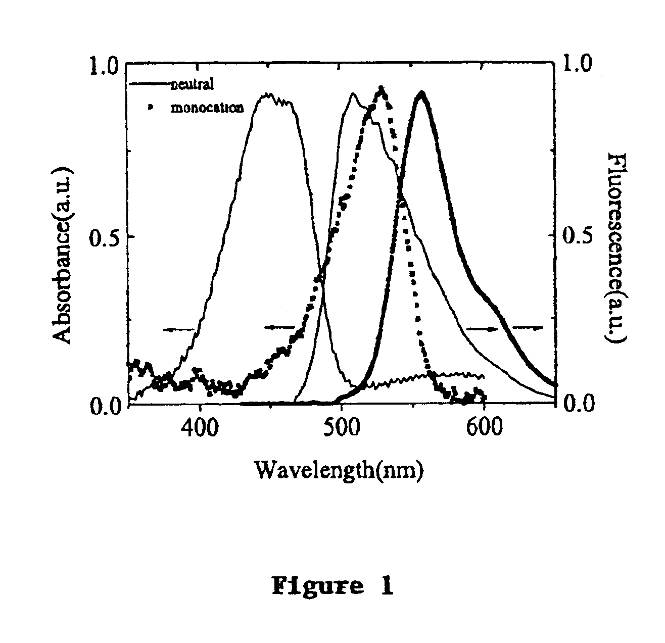
Focus Calibration
A formulation of the same chemically amplified resist as Resist B but doped with 0.05 wt % of the coumarin 6 compound was prepared for focus calibration. Films were coated to a thickness of approximately 0.75 .mu.m onto two 8 in, silicon wafers each pre-coated with an organic antireflective layer and received PABs at 130.degree. C. for 60 seconds. Each of the wafers was exposed with a binary image mask consisting of various features using a GCA XLS 7800 projection lithography system. Since the field of view of the system is much smaller than the wafer area, the exposure was repeated at different positions on each of the wafers as the focus was ramped through a range of 2.4 .mu.m in increments of 0.15 .mu.m (a total of seventeen samples). One of the wafers received a PEE at 130.degree. C. for 90 seconds was developed using an aqueous alkaline developer (Shipley Co.), and underwent SEM analysis. The other wafer underwent fluorescence analysis directly after exposure.
T...
example 3
193 nm Resist
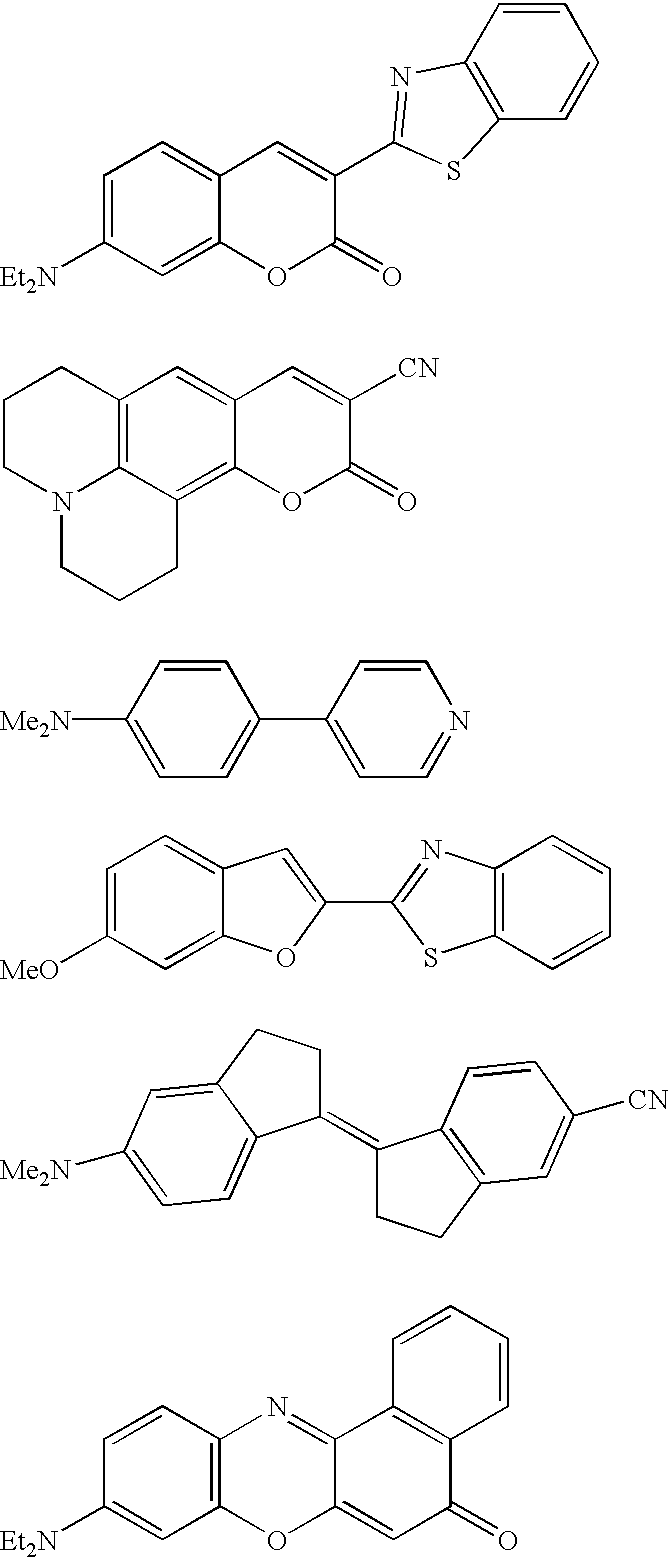
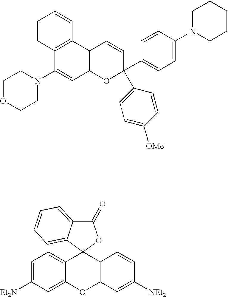
A photoresist containing a resin that contains polymerized units of tetrahydropyran, norbornene, maleic anhydride and 2-methyladamantly methacrylate, a photoacid generator of triphenylsulfonium perfluorobutane sulfonate, a basic additive of tetrabutylammonium lactate, a dye compound of coumarin 6 and a solvent of ethyl lactate was spin-coated onto a silicon wafer substrate, soft-baked and exposed through to patterned 193 nm radiation to provide a latent image of 140 nm features that were visualized by fluorescence through a microscope tool.
PUM
| Property | Measurement | Unit |
|---|---|---|
| wavelengths | aaaaa | aaaaa |
| wavelengths | aaaaa | aaaaa |
| wavelengths | aaaaa | aaaaa |
Abstract
Description
Claims
Application Information