

Semiconductor chip using both polysilicon and metal gate devices
a technology of metal gate and semiconductor, applied in the direction of semiconductor devices, electrical equipment, transistors, etc., can solve the problems of high processing cost, further degradation of device performance, and use of polysilicon ga
- Summary
- Abstract
- Description
- Claims
- Application Information
AI Technical Summary
Benefits of technology
Problems solved by technology
Method used
Image

Examples
Embodiment Construction
According to the present invention, conventional problems are resolved by replacing some of the polysilicon gates with low sheet resistance metal gates. The invention uses specific materials to achieve proper work functions. For example, Ni, TaN, RuO, MoN metal gates are more compatible with P-type doped polysilicon, and Ru Ta TaSi metal gates are more compatible with N-type doped polysilicon.
Thus, according to the present invention, a pure polysilicon gate device is formed in an area where reliability is more important than the performance. Furthermore, according to the present invention, a set of processing steps is utilized that minimizes the process complexity and results in an overall lower processing cost compared with conventional techniques.
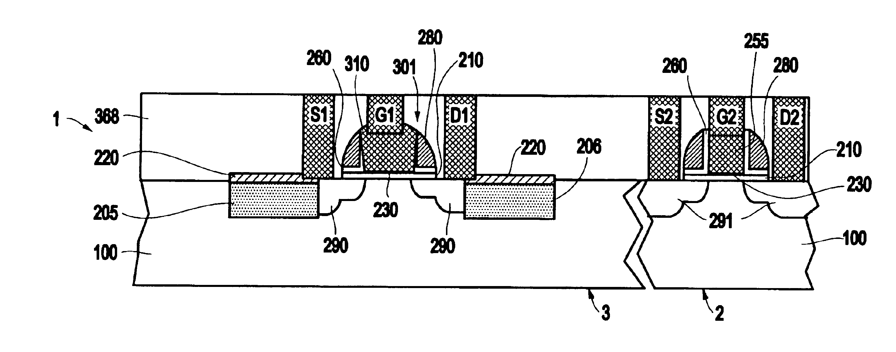
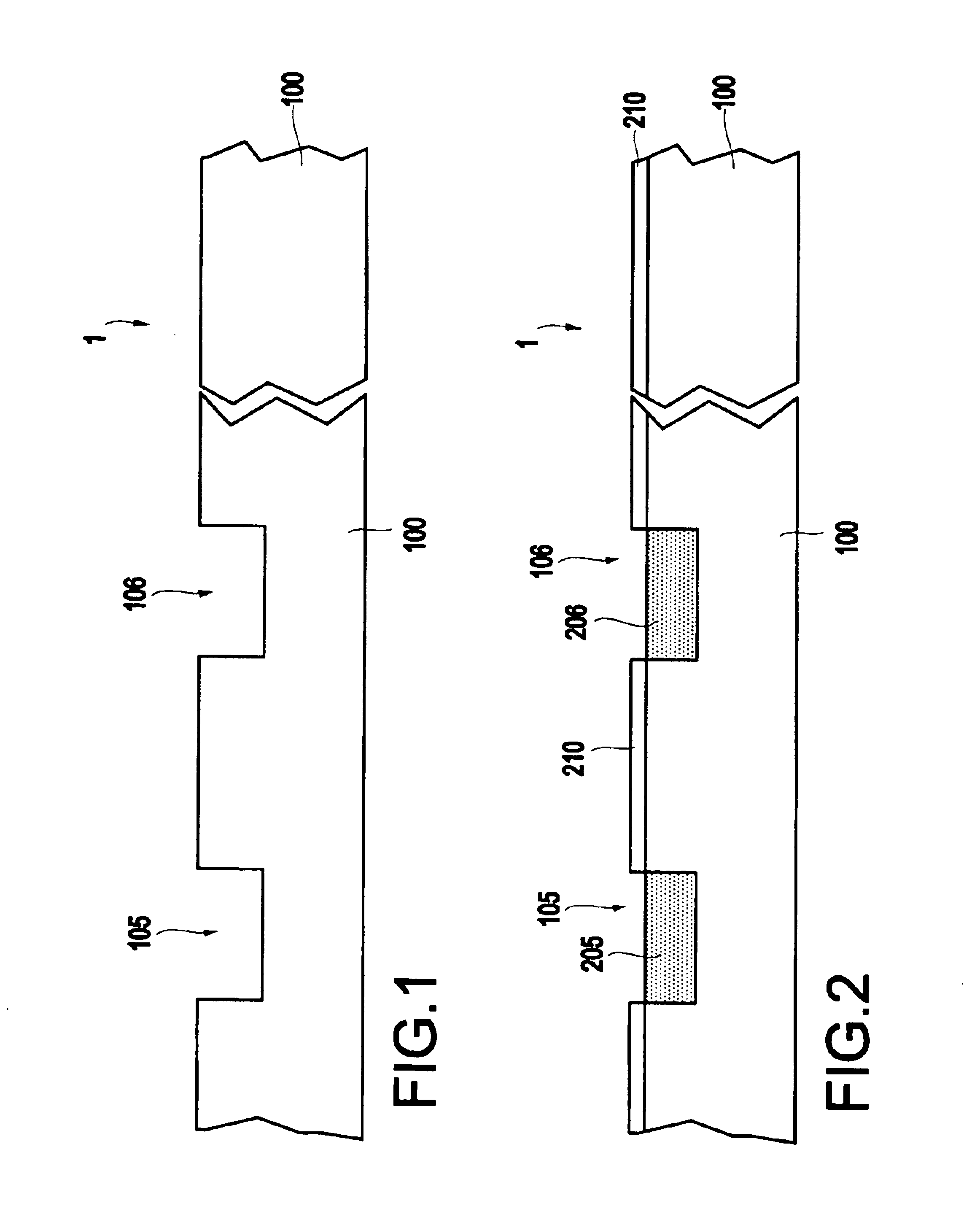
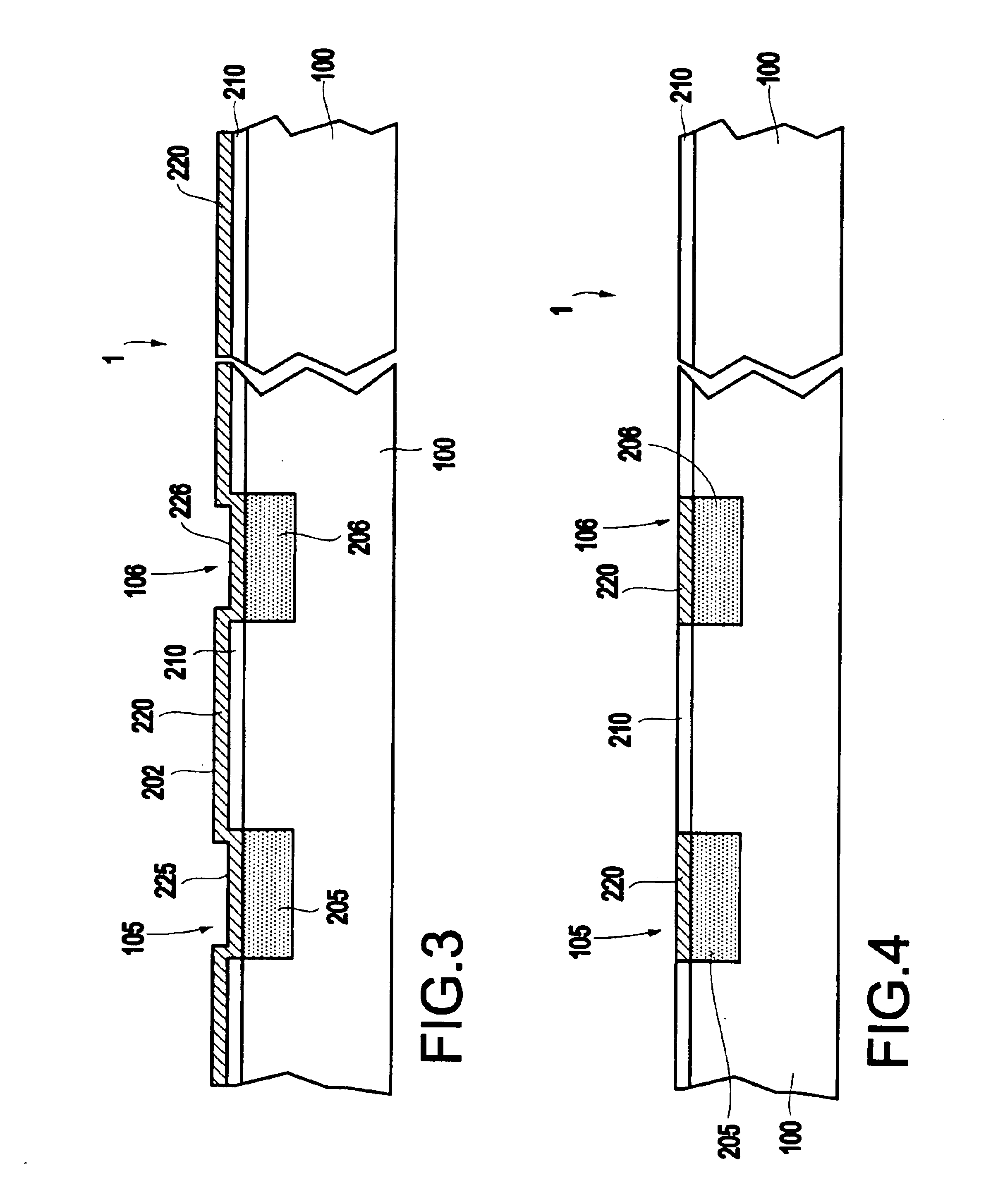
Referring now to the drawings, and more particularly to FIGS. 1 through 15, there are shown preferred embodiments of a semiconductor device 1, and the method of forming the same, according to the present invention. Specifically, as shown ...
PUM
| Property | Measurement | Unit |
|---|---|---|
| temperature | aaaaa | aaaaa |
| areas | aaaaa | aaaaa |
| temperatures | aaaaa | aaaaa |
Abstract
Description
Claims
Application Information