

Method of forming semiconductor wiring structures
a wiring structure and semiconductor technology, applied in the direction of semiconductor devices, semiconductor/solid-state device details, electrical devices, etc., can solve the problems of increasing resistance, increasing resistance value, increasing resistance, etc., and achieve excellent characteristics
- Summary
- Abstract
- Description
- Claims
- Application Information
AI Technical Summary
Benefits of technology
Problems solved by technology
Method used
Image

Examples
Embodiment Construction
Now, embodiments of the present invention will be explained with reference to the drawings.
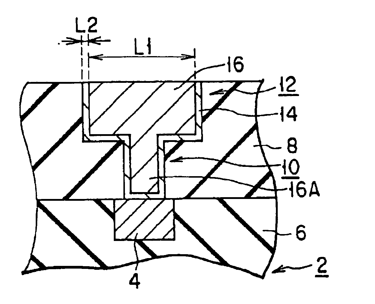
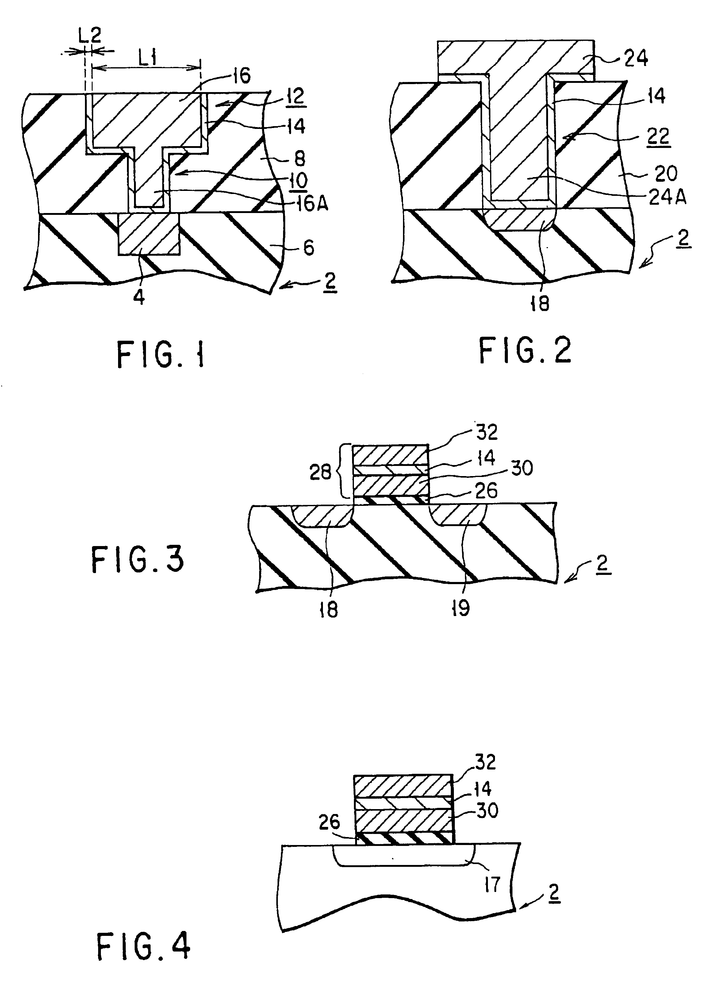
FIG. 1 is an enlarged sectional view showing a barrier metal applied to Cu dual damashine wiring. FIG. 2 is an enlarged sectional view showing a barrier metal applied to a contact hole. FIG. 3 is an enlarged sectional view showing a barrier metal applied to a gate electrode. FIG. 4 is an enlarged sectional view showing a barrier metal applied to a capacitor electrode.
The dual damashine process for forming Cu dual damashine wiring as shown in FIG. 1 is used for the multi-layered structure of wiring to attain a high-performance and multi-functional device in a semiconductor integrated device, namely, a semiconductor integrated circuit. More specifically, in the case where wiring is formed in the multi-layered structure, an upper layer wiring element is connected to a lower layer wiring element. At this time, this process makes it possible to form wiring and via-plug simultaneously, with the resu...
PUM
 Abstract
Description
Claims
Application Information