Semiconductor and fabrication method thereof

Inactive Publication Date: 2005-01-11
SONY CORP
View PDF2 Cites 15 Cited by
  • Summary
  • Abstract
  • Description
  • Claims
  • Application Information

AI Technical Summary

Benefits of technology

An object of the present invention is to provide a semiconductor device capable of increasing the operational speed and reducing the power consumption by providing an nMOS in which the mobility of electrons is increased by a strain effect and a pMOS in which the mobility of positive holes is increased by the strain effect on a common base-substrate, and to provide a method of fabricating the semiconductor device by using the same fabrication process as that used for fabricating a related art CMOS in which the base-substrate is configured as only a silicon substrate.
To achieve the above object, according to a first aspect of the present invention, there is provided a semiconductor device including an n-channel field effect transistor and a p-channel field effect transistor, the both transistors being provided on a common base-substrate, wherein a surface region, in which the n-channel field effect transistor is provided, of the base-substrate includes: a silicon substrate; a buffer layer formed on the silicon substrate, the buffer layer being made from a silicon-germanium compound having a germanium concentration gradually increased toward an upper surface of the buffer layer; a relax layer formed on the buffer layer, the relax layer being made from a silicon-germanium compound having a germanium concentration nearly equal to that of a surface portion of the buffer layer; and a silicon layer formed on the relax layer, and wherein a surface region, on which the p-channel field effect transistor is provided, of the base-substrate, includes: the silicon substrate; a silicon-germanium compound layer formed on the silicon substrate; and a cap layer formed on the silicon-germanium compound layer, the cap layer being made from silicon. In the above-mentioned semiconductor device, source/drain regions of the n-channel field effect transistor may be formed in the silicon layer, and the regions of the p-channel field effect transistor may be formed in the silicon-germanium compound layer.
With this configuration, since the semiconductor device has the CMOS configuration in which the n-channel field effect transistor and the p-channel field effect transistor are provided on the common base-substrate, the power consumption can be reduced. Further, in the n-channel field effect transistor, since the silicon layer is provided on the relax layer made from the silicon-germanium compound whose stress is relaxed because it is formed on the buffer layer, tensile stress is generated in the silicon layer, so that the mobility of electrons is increased by the strain effect due to tensile stress in the silicon layer; and in the p-channel field effect transistor, since the silicon-germanium compound layer is provided on the silicon substrate, compressive stress is generated in the silicon-germanium compound layer, so that the mobility of positive holes is increased due to the strain effect due to the compressive stress in the silicon-germanium compound layer. According to the semiconductor device of the present invention, since the source/drain regions are formed in each of the silicon layer and silicon-germanium compound layer having the above-described unique properties, the operational speeds of the n-channel field e

Problems solved by technology

The technique for making finer device structures, however, has already reached a limitation of a lithography process, in which a pattern having a size smaller than a wavelength of exposure light has been needed to be formed by lithography, and accordingly, at the lithography step, it has come to be difficult to ensure a sufficient process tolerance.
In other words, the attempt to increase the operational speeds of semiconductor devices by making finer device structures is coming closer to a limitation.
Accordingly, while an nMOS transistor having an improved low voltage can be

Method used


Image

  • Semiconductor and fabrication method thereof
  • Semiconductor and fabrication method thereof
  • Semiconductor and fabrication method thereof

Examples


Example

Hereinafter, an embodiment of the present invention will be described with reference to the drawings.

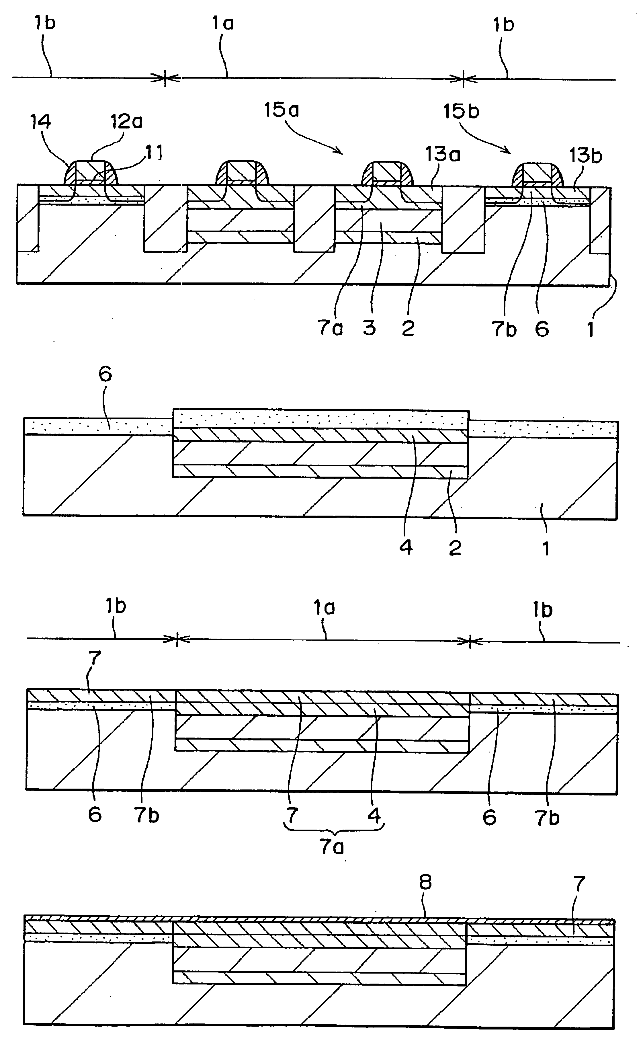
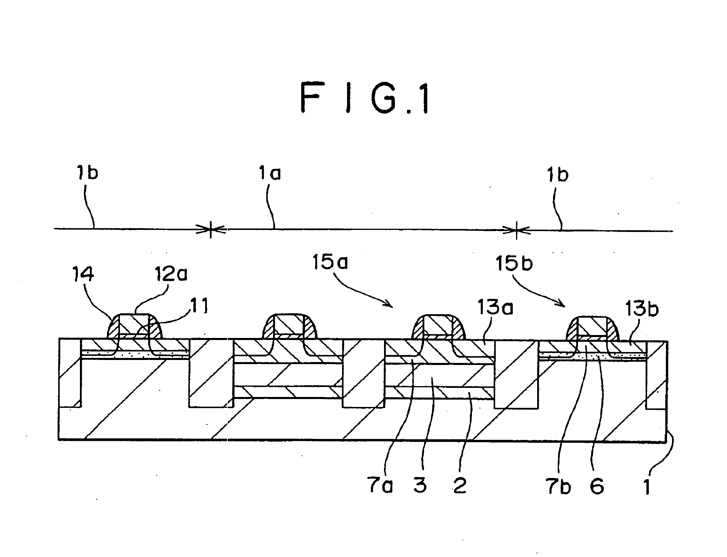
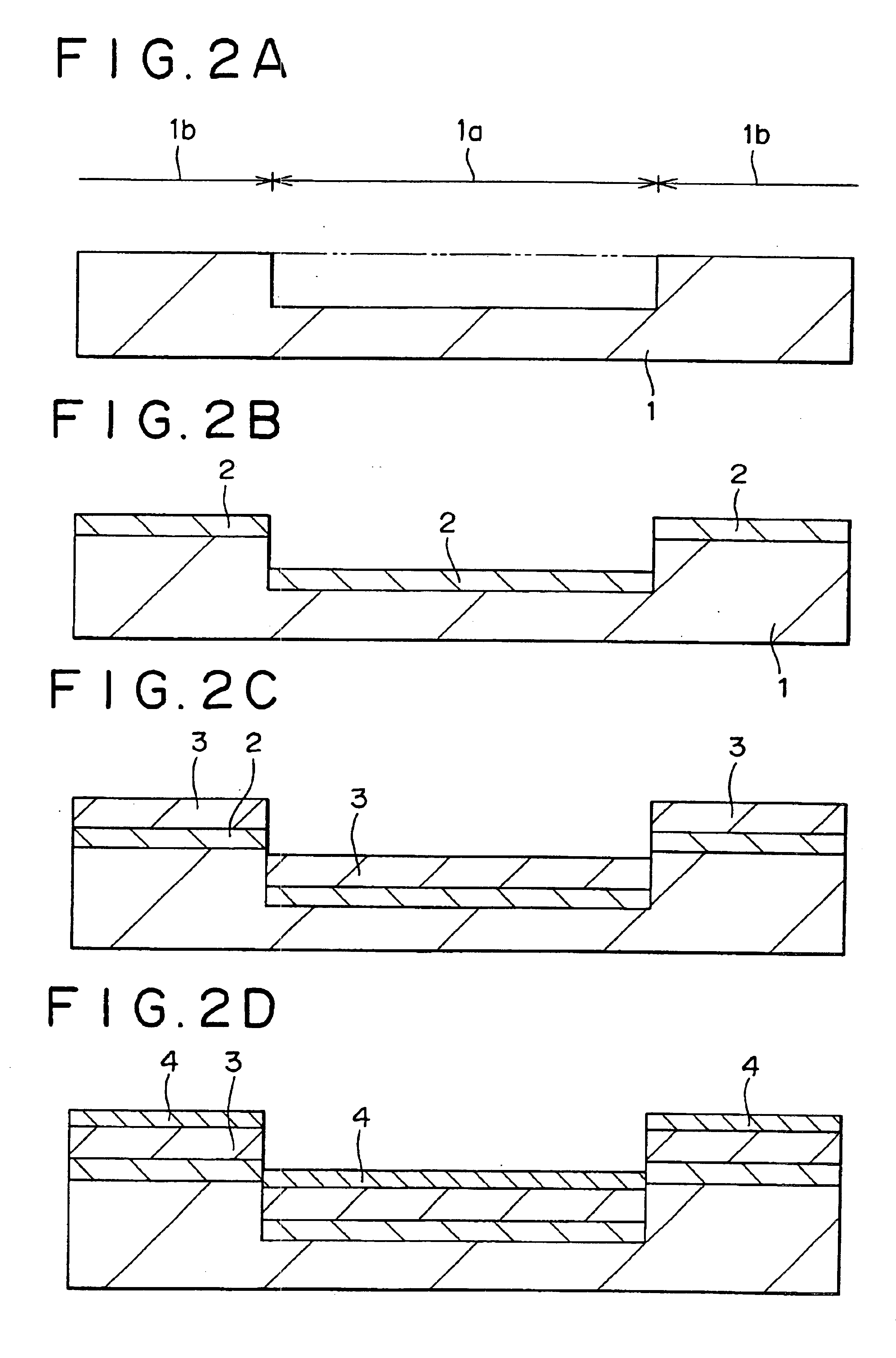
FIG. 1 is a sectional view of a semiconductor device to which the present invention is applied. The semiconductor device has a CMOS configuration in which an n-channel field effect transistor (nMOSTr) 15a and a p-channel field effect transistor (pMOSTr) 15b are provided on a common base-substrate. FIGS. 2A to 6C are sectional views of fragmental structures of the semiconductor device shown in FIG. 1, for illustrating a method of fabricating the semiconductor device.

Referring first to FIG. 2A, a p-type silicon substrate 1 having a diameter of 200 mm, produced by a Czochralski process, is prepared. A resist pattern (not shown) having a thickness of 2.0 μm is formed on the silicon substrate 1 by a lithography process. The resist pattern has an opening portion corresponding to an n-type region 1a on which an nMOSTr is to be formed, and a mask portion corresponding to a p-type region 1b o...


PUM


Abstract

A semiconductor device with p-channel and n-channel field effect devices formed on a common substrate, where the drain and source regions of the n-channel field effect device are formed within a silicon epitaxial layer formed on a silicon layer germanium relax which is formed on a silicon germanium buffer layer with a graduated germanium concentration. Additionally, drain and source regions of the p-channel field effect device are formed within a silicon-germanium compound layer formed on the substrate and the silicon epitaxial cap layer formed on the silicon-germanium compound layer.

Description

BACKGROUND OF THE INVENTIONThe present invention relates to a semiconductor device and a fabrication method thereof, and particularly to a semiconductor device in which an n-channel field effect transistor and a p-channel field effect transistor are provided on a common base-substrate, and a fabrication method thereof.In recent years, along with rapid advance in digitization of information processing means, there have been strong demands to increase the operational speeds of semiconductor devices and to reduce the power consumption of semiconductor devices. Conventionally, the increase in operational speed of semiconductor devices has been achieved by making finer device structures, and the reduction in power consumption thereof has been achieved by adopting semiconductor devices of a complementary type including n-channel and p-channel field effect transistors. The technique for making finer device structures, however, has already reached a limitation of a lithography process, in w...

Claims


Application Information

Patent Timeline
IPC IPC(8): H01L29/66H01L29/02H01L29/10H01L21/70H01L21/8238H01L27/085H01L29/80H01L27/092H01L29/78
CPCH01L21/823892H01L29/802H01L29/1054H01L27/092
Inventor SUGAWARA, MINORUNOGUCHI, TAKASHI
Owner SONY CORP
Why Eureka
Try Eureka