Method and apparatus for slew control of an output signal

a slew control and output signal technology, applied in pulse manipulation, pulse technique, baseband system details, etc., can solve the problems of signal distortion, complex and expensive circuit design, and further deterioration, so as to improve the slew control of output signals and maintain the stability of output signals. , the effect of high quality

Inactive Publication Date: 2005-01-11
AVAGO TECH INT SALES PTE LTD
View PDF10 Cites 31 Cited by
  • Summary
  • Abstract
  • Description
  • Claims
  • Application Information

AI Technical Summary

Benefits of technology

The present invention solves the above and other problems and advances the state of the useful arts by providing apparatus and methods for enhanced slew control of output signals. An output driver receives an input signal and controllably increases the gain of that signal to provide a high quality output signal for use by an electronic device coupled thereto. The output driver may include an operational amplifier that maintains stability of the output signal through a feedback of the output signal. A control circuit supplies a signal to the output of the operational amplifier such that an output transistor turns on more rapidly and improves the shape of the output signal. Once the operational amplifier gains control over the output transistor, the control circuit disengages until needed again. One embodiment of the present invention may be particularly useful as a USB output driver for slow and full speed applications.
In one exemplary preferred embodiment of the invention, a circuit enhances the output signal and includes a driver circuit coupled for receiving a logical input signal and for providing an output signal representative of the input signal such that the output signal is controllable. The circuit also includes a control circuit operating in response to receiving the logical input signal for providing a control signal to the driver circuit to improve the shape of the output signal while the driver circuit substantially maintains control of the output signal.
Another feature of the invention provides a circuit for receiving an input signal and driving an output pad, including: a first switch circuit for applying a first output signal to the output pad in response to receiving a first drive signal; driver circuit for generating a second output signal in response to receiving the input signal; a slew enhancement circuit for generating a third output signal in response to receiving the input signal; and a combiner circuit for combining the second and third output signals for application to the first drive signal to improve a shape of the first output signal.

Problems solved by technology

As the applied signal electronically (or optically) transfers over the medium of the interconnecting bus, some signal distortion may occur.
Often, such distortion may start at the signal generated by the output driver circuit and further deteriorates as the signal traverses the bus structure signal pathway.
Circuit designers often implement complicated and expensive circuits to ensure that the information integrity is maintained or in the alternative to ensure that incorrect data can be detected and corrected.
In other words, the shape of a signal as generated at its source can be an important factor in data integrity problems.
Further, a poorly generated signal shape can be further degraded as it is transmitted over the conductive signal paths of the interconnecting bus structure.
However, present output drivers have failed in delivering “high” quality signals while maintaining lower power requirements.
A problem in delivering a high quality signal from the typical output driver resides in the driver's inadequacy to quickly drive the output transistor.
Unfortunately, the “slew rate” of the operational amplifier is slow in driving the gate of the output transistor.
If the gate voltage of the output transistor rises too slowly, the signal on the output pad may briefly float uncontrolled and hence provide a poorly shaped signal on the output pad.
This brief uncontrolled time for the slew of the output signal results in a poor signal shape at the output pad.
However, such a change to the capacitor affects the stability and power consumption of the output driver.
These approaches may increase power requirements due to large Direct Current (DC) bias currents within the operational amplifier; they may also cause instability problems because of poor settling performance and ringing because of excessive bandwidth of the operational amplifier.
These approaches eliminate the need for a large slewing current but are dangerous because the output transistor will remain undesirably driven at all times. Each of these solutions has unwanted effects that undermine the goals of providing a high quality output signal.
These problems and prior solutions are typical of USB output driver circuits but are also common in other signaling standards and protocols.

Method used


Image

  • Method and apparatus for slew control of an output signal
  • Method and apparatus for slew control of an output signal
  • Method and apparatus for slew control of an output signal

Examples


Embodiment Construction

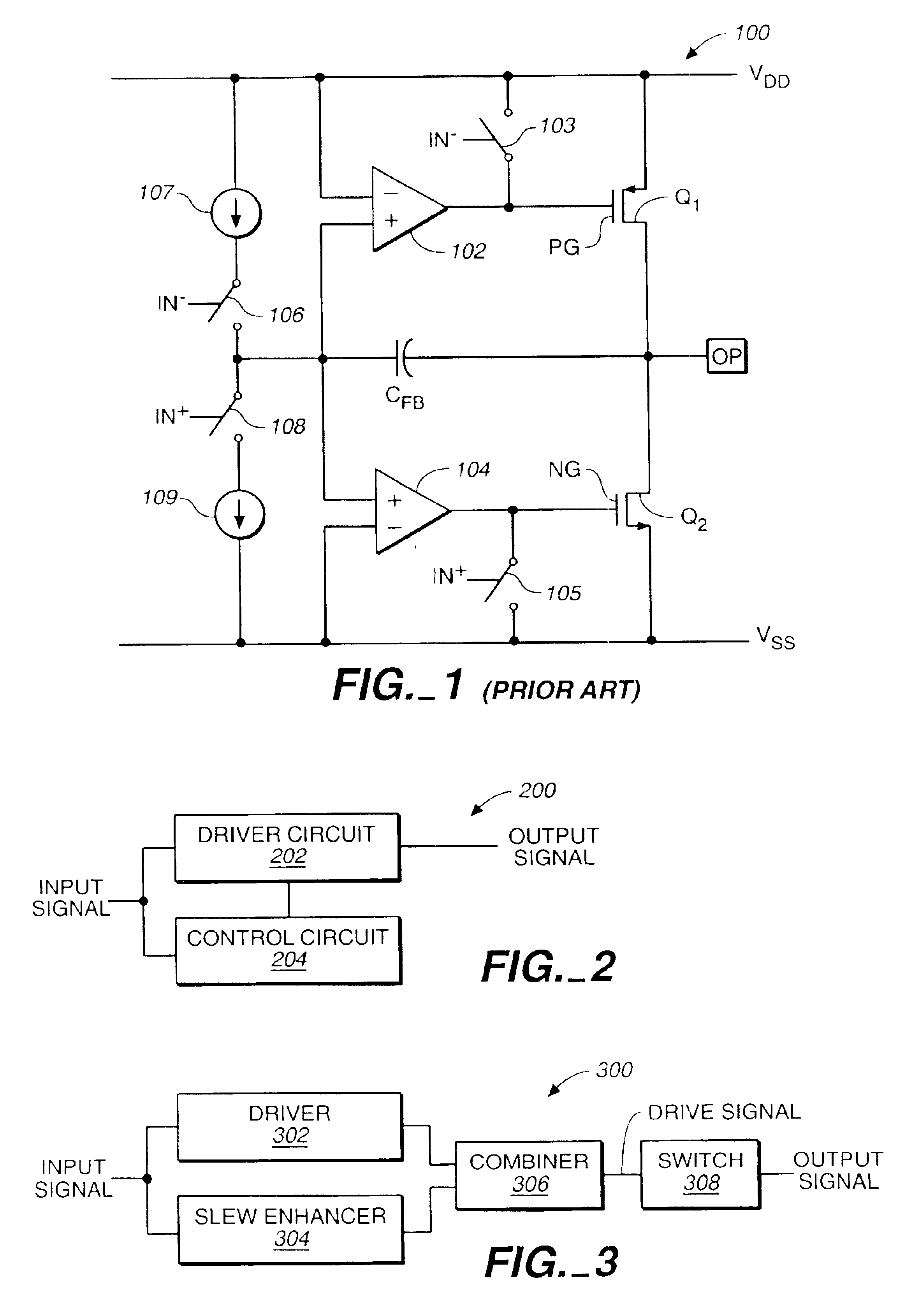
FIG. 1 is a schematic diagram illustrating a prior art output driver circuit.

FIG. 2 is a block diagram illustrating an exemplary preferred embodiment of the invention.

FIG. 3 is a block diagram illustrating another exemplary preferred embodiment of the invention.

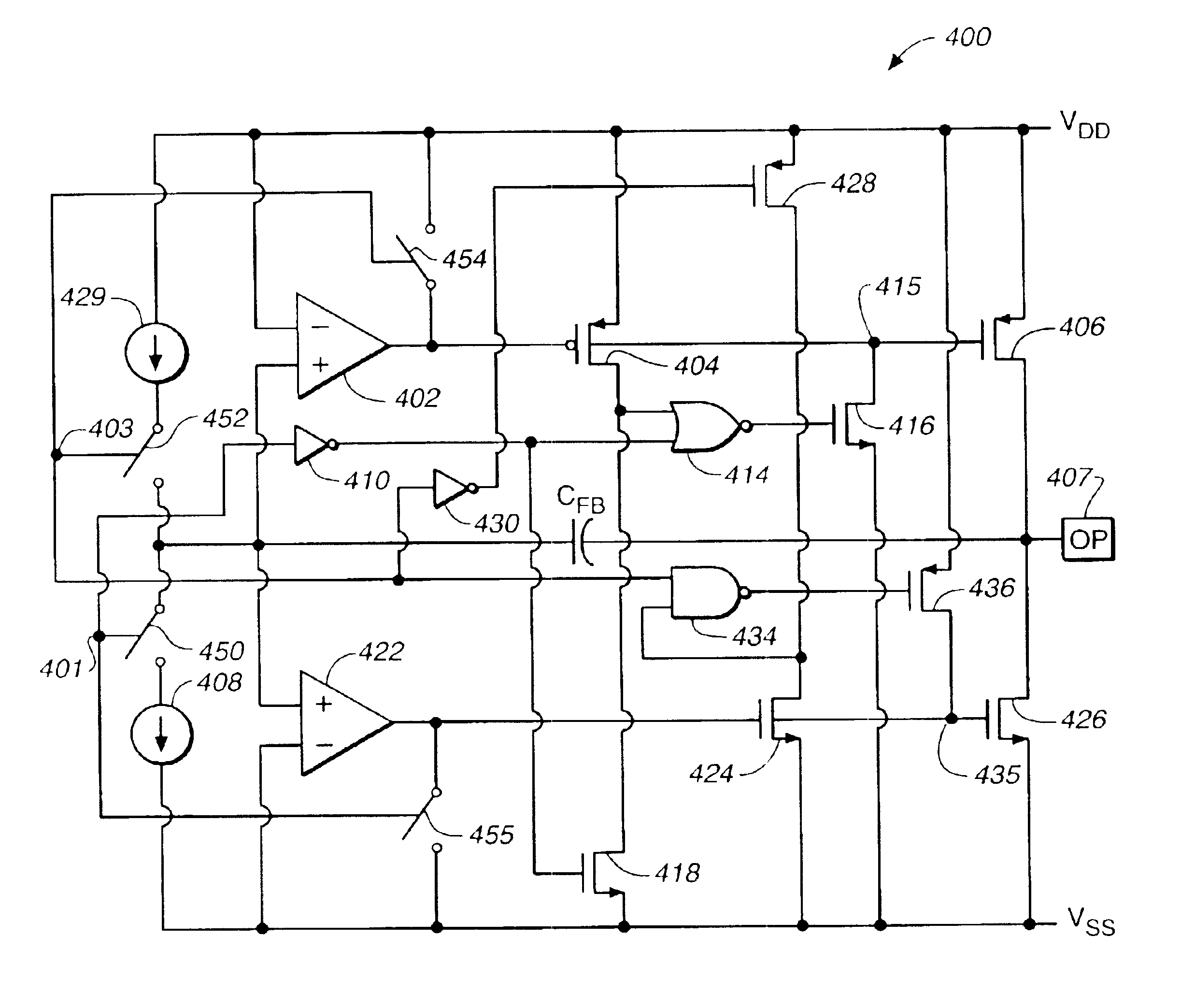
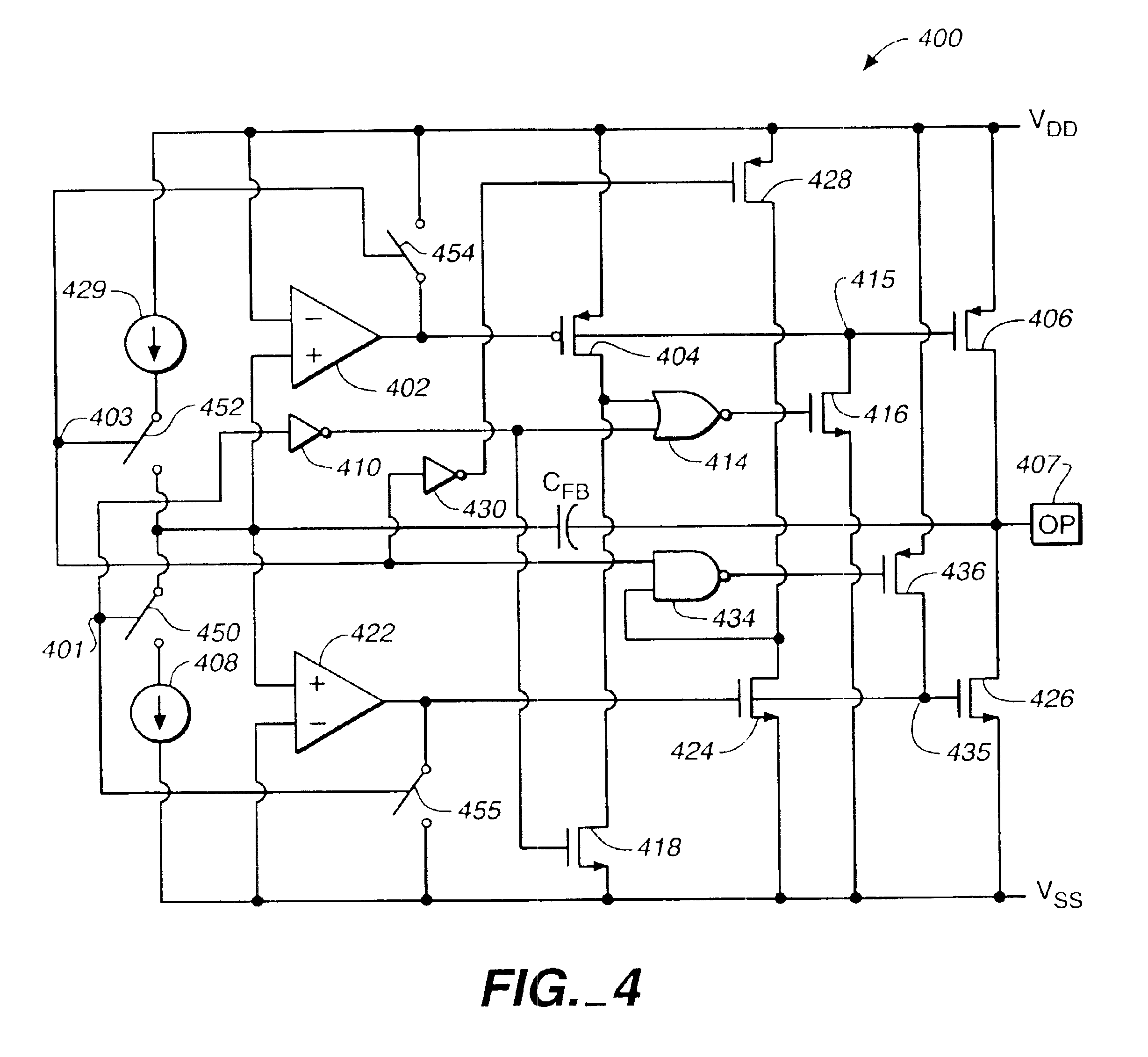
FIG. 4 is a schematic diagram illustrating an exemplary preferred output driver circuit in one embodiment of the invention.

FIG. 5 is a schematic diagram of another prior art output driver circuit.

FIG. 6 is a diagram illustrating a generalized circuit for driving a signal to either of two logic levels as known in the prior art.

FIG. 7 shows timing diagrams of driver circuits described herein.

DETAILED DESCRIPTION OF THE PREFERRED EMBODIMENTS

While the invention is susceptible to various modifications and alternative forms, a specific embodiment thereof has been shown by way of example in the drawings and will herein be described in detail. Those skilled in the art will appreciate that the features described below can be combined ...


PUM


Abstract

Systems and methods for enhancing slew control of output signals. An output driver receives an input signal and controllably increases the gain of that signal to provide a high quality output signal for use by an electronic device coupled thereto. The output driver includes an operational amplifier that maintains stability of the output signal through a feedback of the output signal. A control circuit supplies a signal to the output driver such that the driver to improve the shape of the output signal as the input signal is applied. After the operational amplifier regains control, the control circuit disengages. One embodiment of the present invention may be particularly useful as a USB output driver.

Description

BACKGROUND OF THE INVENTION1. Field of the InventionThe present invention is generally directed toward waveform shaping for input / output devices. More specifically, the present invention relates to controllably enhancing slew of a driver to shape an output signal of the driver.2. Discussion of Related ArtElectronic devices usually exchange signals over a bus structure. A transmitting device applies (or drives) signals onto a bus signal path using an output signal driver circuit and a receiving device receives that signal through a input signal receiver circuit. As the applied signal electronically (or optically) transfers over the medium of the interconnecting bus, some signal distortion may occur. Often, such distortion may start at the signal generated by the output driver circuit and further deteriorates as the signal traverses the bus structure signal pathway.One common bus structure for connecting peripheral I / O devices to a computer system is the Universal Serial Bus. Universa...

Claims


Application Information

Patent Timeline
Patent Type & Authority Patents(United States)
IPC IPC(8): H03K5/04H03K5/12H03K5/01H03K17/16H03K19/017H04L25/02
CPCH03K17/166H04L25/0286H03K19/01707
Inventor MCNITT, JOHN L.RADKE, RUSSELL E.
Owner AVAGO TECH INT SALES PTE LTD
Why Eureka
Try Eureka