Gain block with stable internal bias from low-voltage power supply

a gain block and low-voltage power supply technology, which is applied in the direction of amplifiers with semiconductor devices only, instruments, etc., can solve the problems of affecting the linearity of the amplifier, the battery in the device must be small, and the transmission must be clear, so as to improve the performance and efficiency, the effect of reducing power requirements and prolonging the battery life of portable devices

Inactive Publication Date: 2005-01-11
SKYWORKS SOLUTIONS INC
View PDF84 Cites 53 Cited by
  • Summary
  • Abstract
  • Description
  • Claims
  • Application Information

AI Technical Summary

Benefits of technology

The invention encompasses bias circuit designs that improve performance and efficiency resulting in longer battery life in portable devices due to reduced power requirement and the ability to use power supplies with lower voltages. In particular, the invention encompasses bias circuits implemented with InGaP / GaAs or AlGaAs / GaAs HBTs that are capable of operating from a regulated supply voltage that is as low as about 2.7 V, which is about twice the junction voltage, for instance the base-emitter junction voltage. Preferably, these circuits may be manufactured on a single integrated circuit. The disclosed circuits employ a current mirror configuration to bias gain blocks. Optionally, the gain blocks include transistors arranged in a cascade, such as a Darlington configuration, for high amplification. The invention also encompasses transistors of various other types that may be employed to realize cascaded transistors in gain blocks.
The use of the current mirror configuration enables the use of a low voltage regulated supply or a preferred regulated supply to provide a reference current to a master transistor in the current mirror configuration. The mirrored current, being stabilized by its being proportional to the reference current, then is used to bias one or more transistors powered by a relatively unregulated power supply. Thus, the familiar constraint requiring the power supply voltage to be significantly greater than device voltage in order to provide stable biasing is relaxed resulting in lower resistive losses and improved efficiency.
In another aspect, the invention encompasses providing stability with respect to temperature and process variations by way of feedback provided in current mirror configurations disclosed herein. The invention also encompasses configurations wherein one or more transistors in a cascade configuration are also a part of the current mirror configuration or a feedback loop therein.

Problems solved by technology

Transmissions must be clear and undistorted, and the battery in the devices must be small and have a long life.
Because changes in the DC bias signal affect the operating point of the HBT (and thus adversely affect the linearity of the amplifier), the DC bias signal must be stable and unaffected by variations in temperature or in the power supply voltage.
The approximate current source configurations described above necessarily result in significant resistive losses resulting in low efficiency.
However, this increase in stability is coupled with a reduction in the overall efficiency due to increased resistive losses.

Method used


Image

  • Gain block with stable internal bias from low-voltage power supply
  • Gain block with stable internal bias from low-voltage power supply
  • Gain block with stable internal bias from low-voltage power supply

Examples


Embodiment Construction

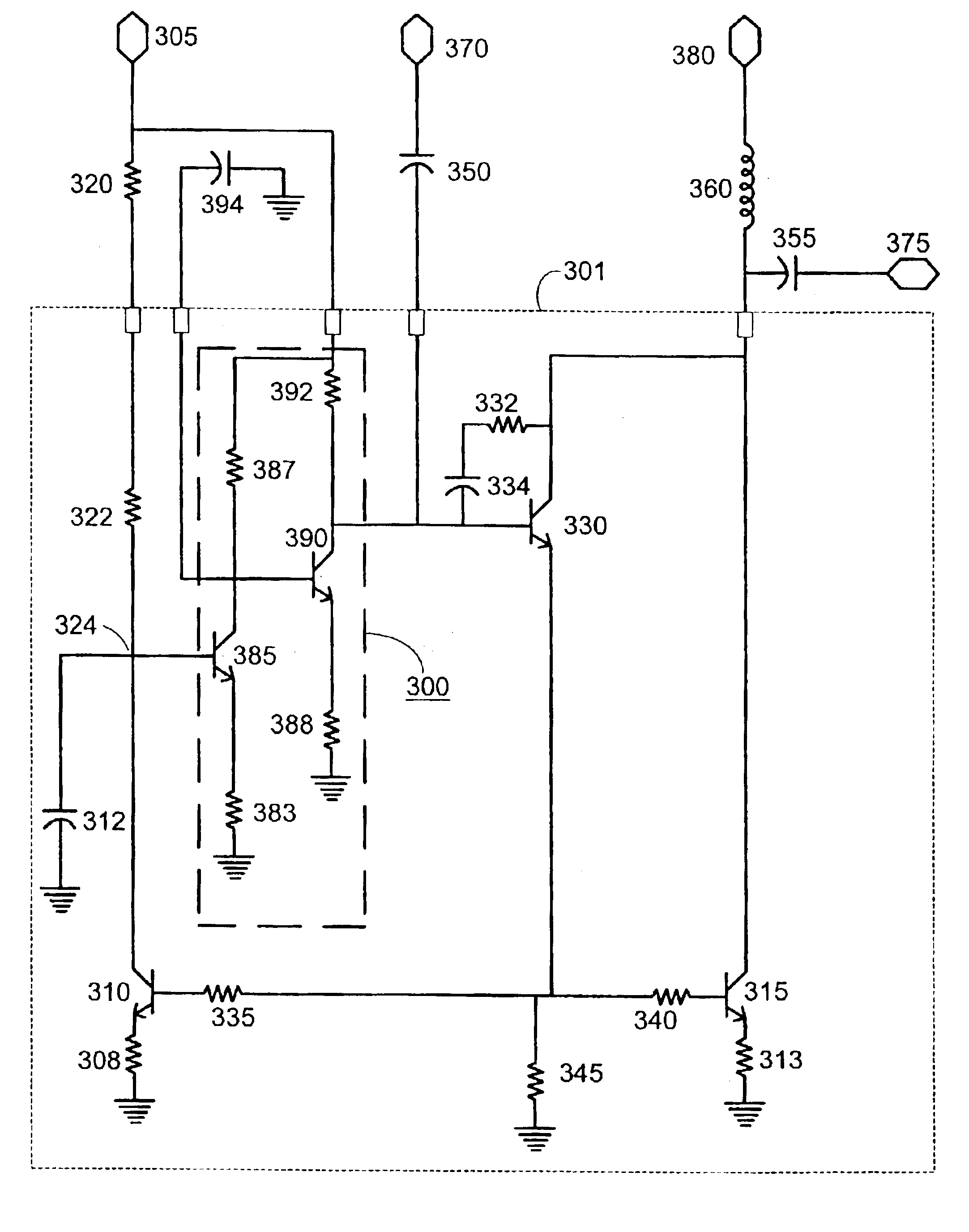
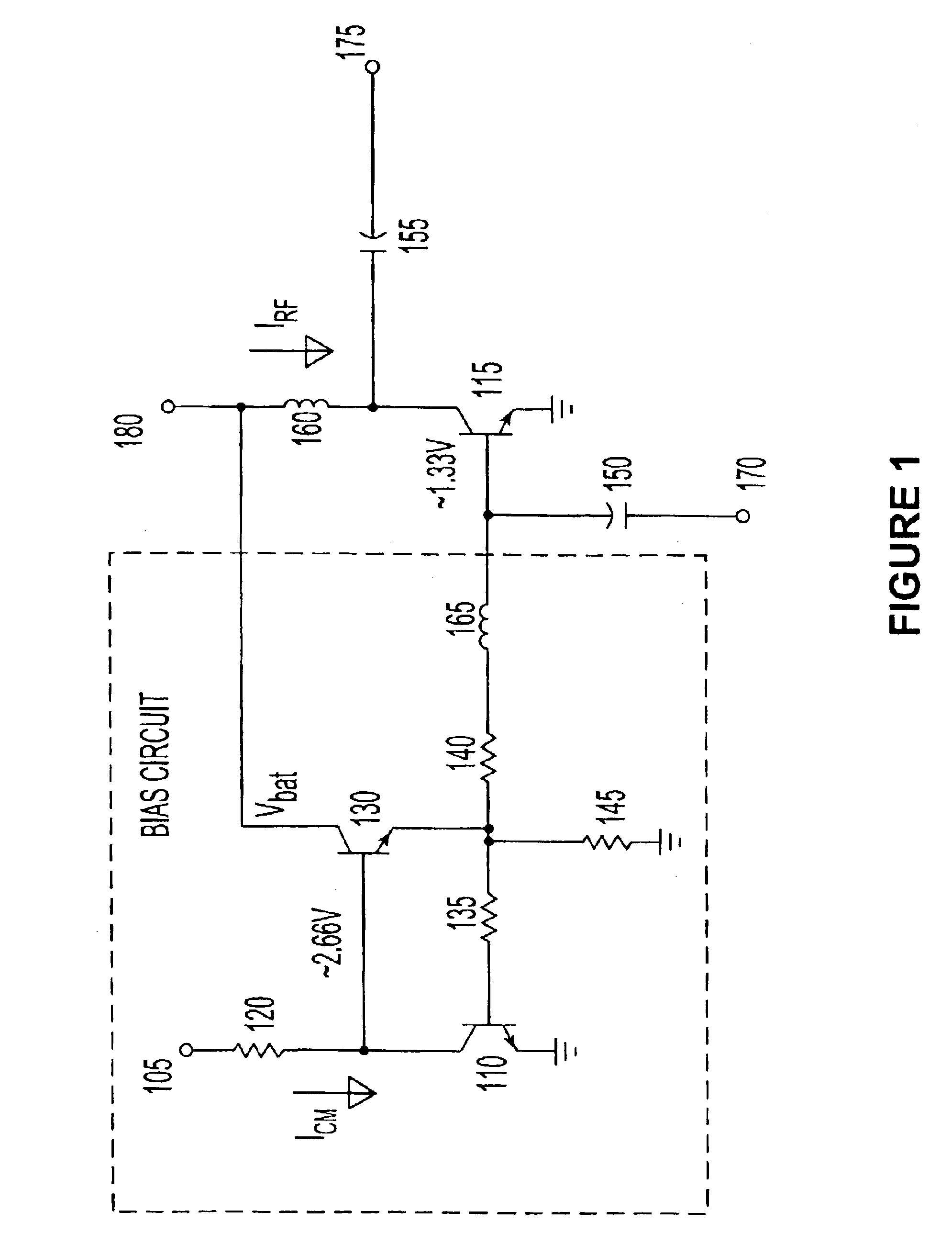
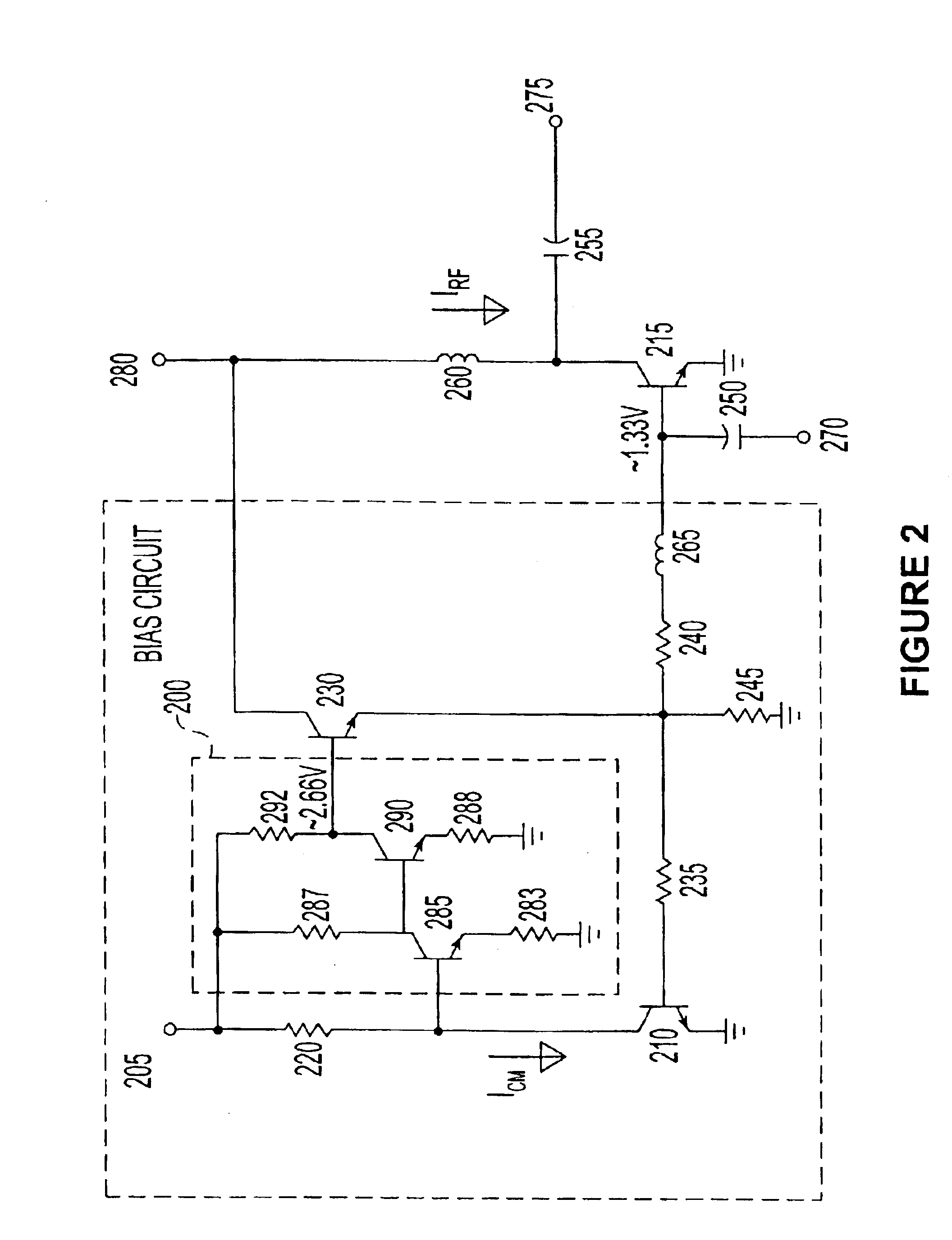
In general, the illustrative circuits described in FIGS. 1-4 may be used to bias a one or more transistor. A regulated low voltage supply terminal provides a reference current to a master transistor in a current mirror configuration. The mirrored current to a second transistor in the current mirror configuration serves as a suitable biasing current. The second transistor, biased by the current mirror arrangement, may concurrently be in a cascade arrangement of transistors. A power supply, including unregulated power supplies, may be connected to an output terminal with suitable isolation from the output signal, to provide the biasing current in accordance with a mirror current to the second transistor in the current mirror configuration. The cascade arrangement of transistors, when present, may be used to provide high gain to an input signal. The described arrangement is preferably further stabilized by a feedback circuit comprising an amplifier to counteract variations at a current...


PUM


Abstract

A transistor bias circuit is provided that is capable of operating from a power supply voltage that is slightly higher than twice the base-emitter voltage of the transistor to be biased. The bias circuit includes a transistor connected in a current-mirror configuration with the transistor to be biased. A feedback circuit maintains the mirrored current at a constant level. The gain of the feedback circuit is improved by the addition of a non-inverting amplifier within the feedback circuit. In a preferred embodiment, the biased transistor is concurrently in both a Darlington and the current mirror configuration. Moreover, a feedback transistor in the feedback circuit is also concurrently in the Darlington configuration, thus providing an efficient biasing arrangement for an amplifier block based on the Darlington arrangement.

Description

FIELD OF THE INVENTIONThe present invention relates generally to a circuit for biasing a gain block using a large unregulated power supply with the aid of a low-power stable power supply for increased efficiency in the operation of the gain block.BACKGROUND OF THE INVENTIONModern wireless communications devices, such as cellular telephones, are held to ever-higher performance standards. Transmissions must be clear and undistorted, and the battery in the devices must be small and have a long life. In order to meet these consumer requirements, wireless telephone designers have moved away from using traditional silicon-based bipolar transistors as power amplifiers and toward using more exotic transistors, such as heterojunction bipolar transistors (“HBTs”) made of aluminum-gallium-arsenide / gallium-arsenide (“AlGaAs / GaAs”), indium-gallium-phosphide / gallium-arsenide (“InGaP / GaAs”), InGaP / GaAsN, and double heterojunction bipolar transistor (DHBT) in an non-exhaustive listing. Such HBTs pr...

Claims


Application Information

Patent Timeline
Patent Type & Authority Patents(United States)
IPC IPC(8): G05F3/08G05F3/26H03F3/343H03F1/30
CPCG05F3/265H03F3/343H03F1/302H03F2200/513
Inventor JOHNSON, DOUGLAS M.LIWINSKI, HENRY Z.
Owner SKYWORKS SOLUTIONS INC
Why Eureka
Try Eureka