Method of manufacturing a spark plug for an internal combustion engine
a technology for internal combustion engines and spark plugs, which is applied in the manufacture of spark plugs, sparking plugs, agriculture, etc., can solve the problems of affecting the service life of the spark plug, so as to achieve the effect of reducing the thermal stress of the molten bond, high bonding strength and high durability
- Summary
- Abstract
- Description
- Claims
- Application Information
AI Technical Summary
Benefits of technology
Problems solved by technology
Method used
Image
Examples
first embodiment
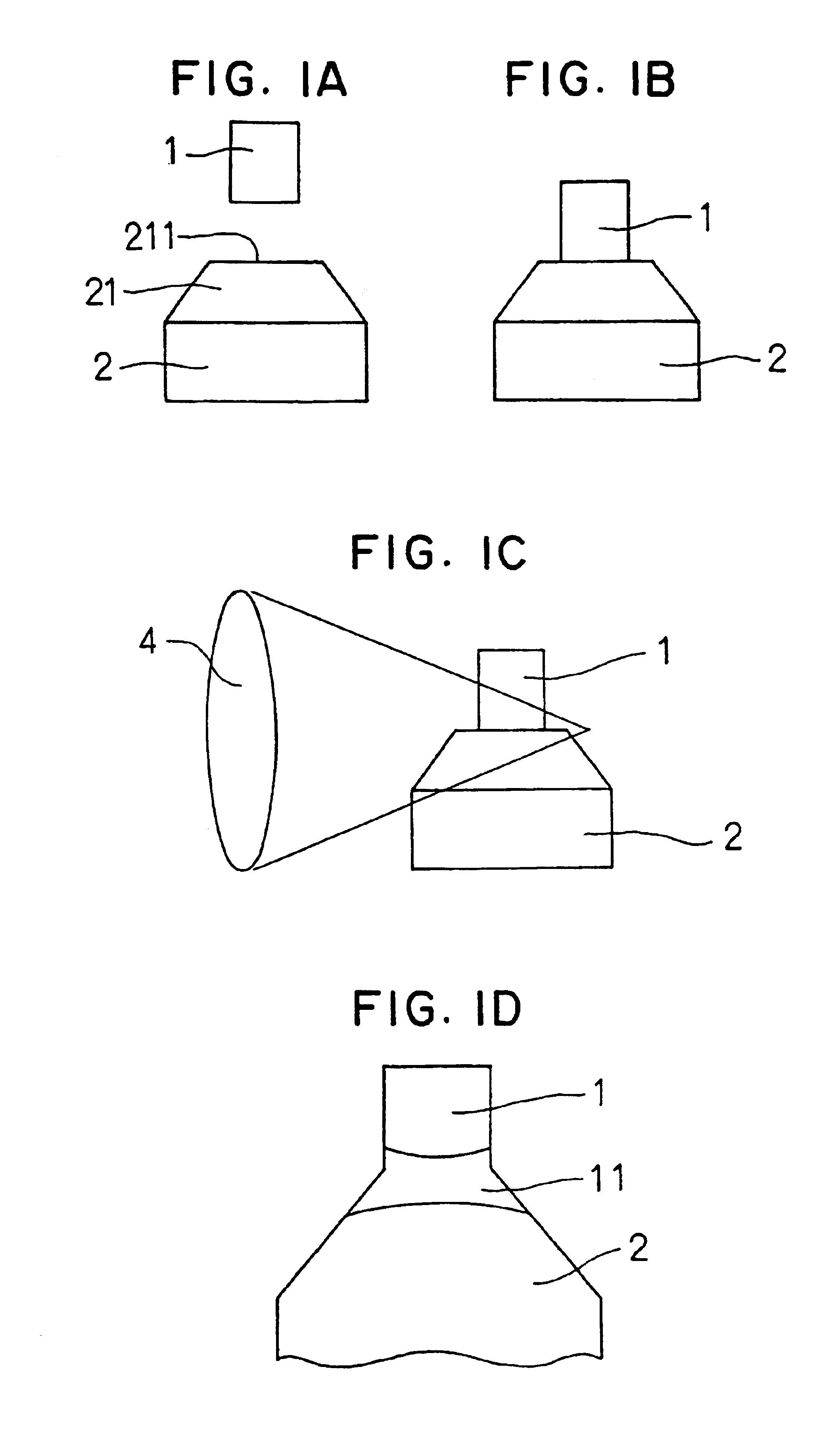
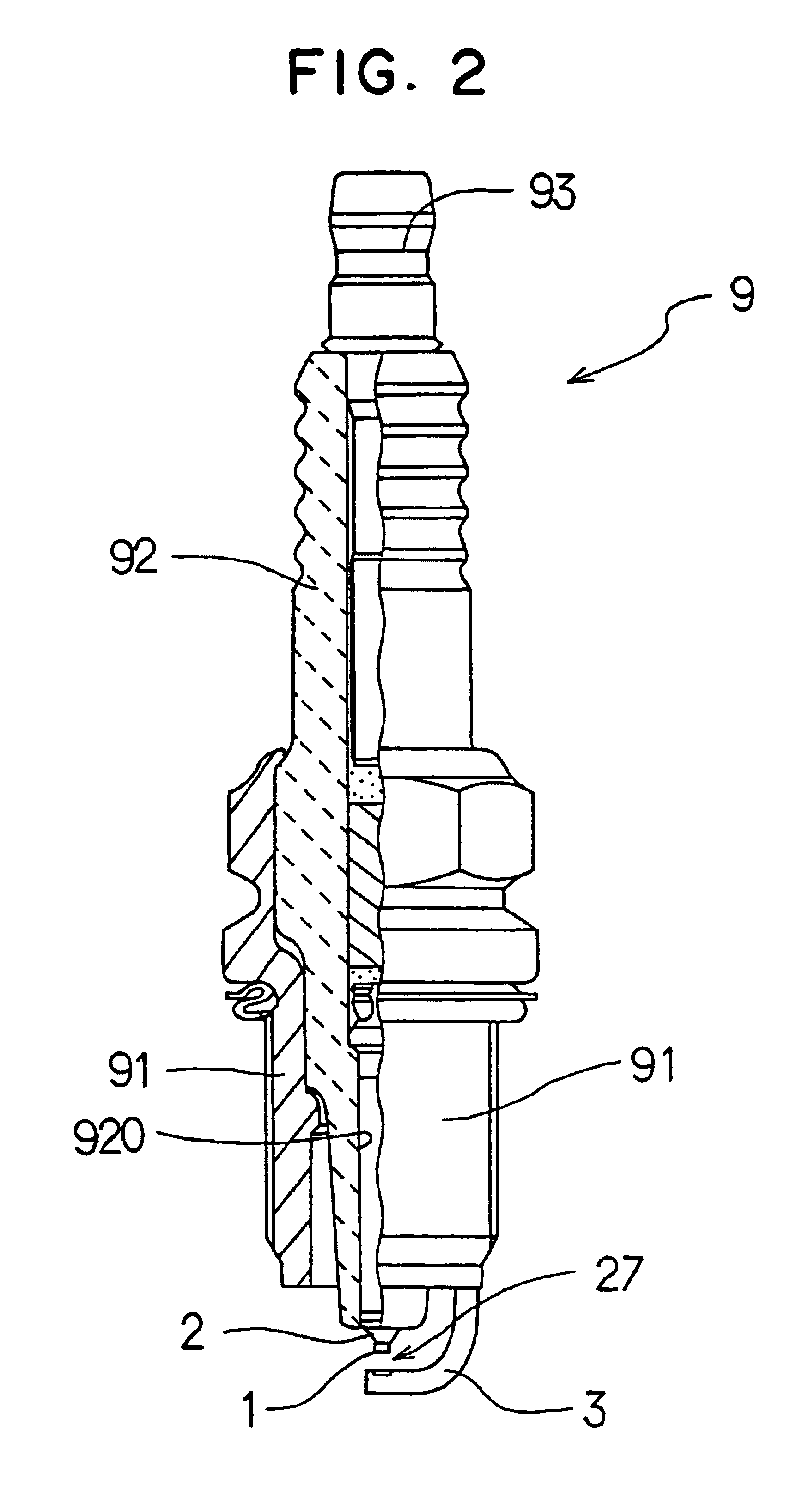
Referring to FIGS. 1 to 8, a first embodiment according to the present invention will be described. FIG. 2 shows spark plug 9 for an internal combustion engine to which the present invention is applied, and FIG. 3 shows a part of the spark plug including center electrode 2 to which noble metal chip 1 is welded. Referring to FIG. 2, spark plug 9 is composed of insulator 92 having through hole 920 therein, center electrode 2 disposed at the bottom end of through hole 920, metal housing 91 which holds insulator 92 therein, ground electrode 3 attached to metal housing 91 and disposed to face center electrode 2, and terminal 93 for connecting the spark plug to a high voltage source. Center electrode 2 and ground electrode 3 constitute spark gap 27. On the tip of center electrode 2, noble metal chip 1 is bonded by laser welding.
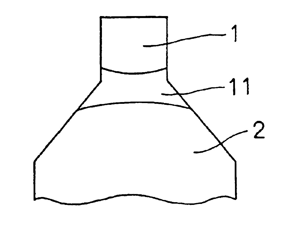
Referring to FIG. 1D, noble metal chip 1 made of an Ir (iridium) alloy having a melting point higher than 2,200° C. is welded to center electrode 2 with molten bon...
second embodiment
A second embodiment according to the present invention will be described, referring to FIGS. 9A, 9B, 9C and 10. In this embodiment, noble metal chip 10 made of Ir containing no Rh is used, and rhodium (Rh) chip 15 is placed between noble metal chip 10 and center electrode 2 so that Rh is melted into molten bond 150 by laser welding. As shown in FIG. 9A, Rh chip 15 is placed on end surface 211 of center electrode 2 and preliminarily connected to it by resistance welding. Then, as shown in FIG. 9B, noble metal chip 10 is placed on Rh chip 15 and preliminarily connected to it by resistance welding. The laser beam having energy of 7.5 J is radiated and focused on the periphery of Rh chip 15 to form molten bond 150 in the same manner as in the first embodiment. Noble metal chip 10 and center electrode 2 are welded together with molten bond 150 interposed therebetween as shown in FIG. 9C. Molten bond 150 is an alloy containing Rh, Ir (material of noble metal chip 10) and Ni (material of c...
third embodiment
A third embodiment according to the present invention is shown in FIGS. 11 and 12, in which molten bond 11 includes unmolten portion 116 at its center. In this embodiment, the junction of noble metal chip 1 and center electrode 2 are welded together by the laser beam only at its periphery, leaving unmolten portion 116 at its center as shown in FIG. 11. If the thickness T in which more than 1 wt % of Rh is contained in molten bond 11 is thicker than 0.2 mm, noble metal chip 1 and center electrode 2 are securely bonded, the thermal stress in the molten bond being sufficiently small. The thickness T is measured at a position apart from center line P by distance S which is a half of radius R of noble metal chip 1, as shown in FIG. 11. In an example shown in FIG. 12, Rh chip 15 is disposed between noble metal chip 10 and center electrode 2 as in the second embodiment, and a part of Rh chip 15 is left unmelted while its peripheral part is melted to form molten bond 11. In this case too, i...
PUM
 Abstract
Description
Claims
Application Information


